|
This section describes advanced features and special functions provided with the BAE PCB design system.
4.6.1 Batch Design Rule Check, Report
The
function from the Layout Editor
menu is used to run a complete design rule check on the currently loaded layout. It is strongly recommended to use
before generating CAM data and/or passing CAM data to the PCB manufacturer to avoid design rule violations such as short-circuits, unrouted nets or clearance violations. Use the following commands to perform a batch design rule check on the currently loaded layout
board of the
demo.ddb DDB file:
| Utilities |  |
| Batch DRC | |
| Please confirm (Y/N) ? | y  |
After performing the design rule check, the
function implicitly activates the
function from the
menu to display the checking results and the design state. The
function can also be called explicitly using the following commands:
| Utilities | |
| Report | |
The following listing is displayed by the
function or after
(zero error lines might be omitted):
File : demo.ddb
Type : Layout / Element : board


Number of Nets .................: 22
Number of Open Connections .....: 0
Number of Short Circuits .......: 0
Copper Distance Violations .....: 0
Documentary Distance Violations : 0
Number of Power Layer Errors ...: 0
Number of Missing Parts ........: 0
Number of Wrong Type Parts .....: 0
Number of Missing Netlist Pins .: 0
Height Distance Violations .....: 0
Power Layers in Use.............: -
Signal Layers in Use............: 1-2
The
Number of Nets report entry displays number of nets defined in the net list of the currently loaded layout. The
Number of Open Connections entry denotes the number of not yet routed (two-point) connections on the currently loaded layout. The
Number of Short Circuits entry denotes the number of short-circuits encountered by the Design Rule Check. The
Copper Distance Violations entry denotes the number of copper layer clearance distance violations online-encountered by the Design Rule Check on the currently loaded element. The
Documentary Distance Violations entry denotes the number of clearance distance violations on documentary layers. The
Number of Power Layer Errors entry denotes number of copper area cross-intersections on split power planes. The
Number of Missing Parts report entry denotes the number of net list parts not yet placed on the currently loaded layout. The
Number of Wrong Type Parts report entry denotes the number of net list parts placed with a wrong part package type (macro) on the currently loaded layout. The
Number of Missing Netlist Pins entry denotes the number of unplaced and/or missing net list pins. Missing net list pins can cause an erroneous open connections count. An indicator is added to the open connections count if net list pins are missing. The
checklnl User Language program can be used to track missing net list pins.
The
Height Distance Violations entry denotes the number of (part) height design rule violations.
The
Power Layers in Use and
Signal Layers in Use report entries display the used power and signal layers. Signal layer 1 to top layer are always assumed to be in use. These entries help to identify power layers without global net assignment, hence with split power planes to be considered by connectivity.
DRC Error Display
The
dialog from the Layout Editor
menu provides the
parameter for selecting DRC distance and height rule violation error display modes and/or colors. The
option displays error boxes using the error color selected with the
function, the default of which is white. The
setting displays error rectangles using the color selected for the layer on which the erroneous element is placed. Errors on layers which are faded-out through
are not displayed.
The
Layout Editor
menu provides the
function for displaying the DRC distance and height rule violation error lists. The DRC errors are listed in a popup menu, indicating error type, error layer and error coordinates for each error. A
to the error position ist triggered when selecting an error from the list using the left mouse button. The
+ and
- keys can be used to move the zoom window through the error position list in either direction.
Note that the modified
BAE HighEnd data structure for storing the layout connectivity data allows for a selective shortcut display, i.e., shortcuts between two nets are displayed by highlighting only those elements causing the shortcut, whilst
BAE Professional highlights the whole connection tree affected by the short-circuit.
Hit the spacebar to return to the
Layout Editor menu.
4.6.2 Color Setup, Color Tables, Pick Preference Layer
The
function from the
menu activates a popup menu for modifying the current color settings. This color setup menu simultaneously can be utilized for displaying the current color assignments. Changing some item-specific color is accomplished by selecting the desired display item using the left mouse button and then selecting the desired color button from the
function. In the layout system,
provides a feature for fast display item fade-out/fade-in. Activating and/or deactivating some item-specific display is accomplished by selecting the desired display item entry with the right mouse button which works as a toggle between fade-out and fade-in. The system won't loose information on currently defined colors of faded-out display items; strike-through color buttons are used for notifying currently faded-out display items.
At overlaps of different elements the resulting mixed color is displayed. The highlight color is also mixed with the color of the element to be marked, thus resulting in a brighter display of that element.
The
function from the
menu is used to save the current color settings with a user-specified name to the
ged.dat system file in the BAE programs directory. When starting the
Layout Editor (or any other layout program module), the color table named
standard is automatically loaded. Any other color table available in
ged.dat can be loaded using the
function from the
menu.
It is a good idea to define color tables for certain tasks such as
stackdef for padstack editing (i.e., with drill holes and drill plan visible) or
unroutes for fast open connections recognition (i.e., with airlines visible only). At the definition of color tables it is to be considered that screen redraw functions will take longer if more objects must be displayed. It is recommended to define task-specific color tables to display only those objects which are important for the corresponding task.
The
function is usually used to allow selection on a specific layer. It also has the useful hidden function of loading a layer-specific color table. These color tables have specific names, and if they don't exist there will be no change in the color display. See
table 4-3 for the color table names assigned to the pick preference layers
(<n> is the layer number, respectively).
Table 4-3 also lists short layer names which can optionally be used in certain layer menus for selecting layers via keyboard input.
Table 4-3: Pick Preference Layer Color Tables and Short Layer Names
| Layer | Pick Preference Layer
Color Table Name | Short
Layer Name |
|---|
| Signal Layer <n> | layer_<n> | <n> |
| Signal Layer All Layers | layer_all | a |
| Signal Layer Middle Layers | layer_def | m |
| Signal Layer Top Layer | layer_def | |
| Power Layer <n> | | p<n> |
| Documentary Layer <n> Side 1 | layer_d<n>_1 | d<n>s1 |
| Documentary Layer <n> Side 2 | layer_d<n>_2 | d<n>s2 |
| Documentary Layer <n> Both Sides | layer_d<n>_a | d<n>sa |
| Board Outline | | b |
| Airlines | | u |
When selecting a certain pick preference layer (e.g., signal layer 2) using the
function, the color table with the corresponding name (e.g.,
layer_s2) is automatically loaded if available in
ged.dat. This feature is most useful for e.g., manual routing.
4.6.3 Layout Net List Changes
The Layout Editor provides functions for performing pin/gate swaps to simplify the routing problem. Alternate package types can be assigned to layout parts, and net list part names can be changed for better legibility of the insertion plan (for manual insertion). These modifications are net list changes which must be backward annotated to the schematics using the
function from the
Schematic Editor (see also
chapter 3.3).
In this section we will apply some pin/gate swaps and change a couple of part names. First of all, use the following commands to set the coordinate display mode to inch and apply group functions to delete all traces from the currently loaded layout:
| Settings | |
| Coordinate Display | |
| Display Inch | |
| Groups | |
| Group Polygon | |
| Traces | |
| Select | |
| Move to [0.1",0.1"] | |
| Move to [2.8",0.1"] | |
| Move to [2.8",2.7"] | |
| Move to [0.1",2.7"] | |
| Done | |
| Delete Group | |
The
function from the
menu is used to perform manual pin/gate swaps. Use the following commands to swap the pins
1 and
2 of the switches named
s1000,
s1001,
s1002 and
s1003, respectively:
| Parts | |
| Pin/Gate Swap | |
| Move to "s1000.1",[0.2",2.3"] | |
| Move to "s1000.2",[0.5",2.3"] | |
| Pin/Gate Swap | |
| Move to "s1001.1",[0.2",2.1"] | |
| Move to "s1001.2",[0.5",2.1"] | |
| Pin/Gate Swap | |
| Move to "s1002.1",[0.2",1.9"] | |
| Move to "s1002.2",[0.5",1.9"] | |
| Pin/Gate Swap | |
| Move to "s1003.1",[0.2",1.7"] | |
| Move to "s1003.2",[0.5",1.7"] | |
Note how the
function provides graphical pin/gate swap indicators. A circle (0.6mm diameter,
color) is displayed for every pin/gate swap enabled pin when the
function is activated. The indicator for the first selected pin turns into a filled square, leaving only swappable pins marked by circles and character codes for the possible swap operations. The character codes are
P for pin swap,
G for gate swap and
A (Array) for gate group swap. Selecting black for the
color deactivates the pin/gate swap indicator display.
Each pin/gate swap is performed using the corresponding pin/gate swap definition from the Logical Library (see also
chapter 7.11 for a description of the
loglib utility program and
chapter 3.2 for a description of the
Packager program module). The following error message is issued if no swap is allowed for the selected pins and/or gates:
Not allowed to swap these pins!
Use the following commands to swap the gates (1,2,3) and (5,6,4) as well as the pins
12 and
13 of the part named
IC10:
| Parts | |
| Pin/Gate Swap | |
| Move to "ic10.(1,2,3)",[1.4",1.8"] | |
| Move to "ic10.(5,6,4)",[1.5",1.8"] | |
| Pin/Gate Swap | |
| Move to "ic10.12",[1.4",2.1"] | |
| Move to "ic10.13",[1.3",2.1"] | |
Use the following commands to perform a part swap for the resistor parts named
R101 and
R103 (this is allowed because the same attribute values are assigned to these parts):
| Parts | |
| Pin/Gate Swap | |
| Move to "r101",[1.6",2.4"] | |
| Move to "r103",[1.4",1.2"] | |
The
function from the Parts menu is used to change part names in the net list. Use the following commands to change the net list part name of connector
X1000 to
filenameX1, and also change the net list part name of diode
V1000 to
V2:
| Parts | |
| Netlist Part Name | |
| Move to "x1000",[2.4",1.5"] | |
| Part Name (X1000) ? | X1 |
| Netlist Part Name | |
| Move to "v1000",[1.2",1.2"] | |
| Part Name (V1000) ? | V2 |
The
function issues the following error message if you try to assign a part name which is already in use for another part:
Part name already in use!
Use the following commands to apply the
function to change the name of part
IC10 to
IC1:
| Parts | |
| Change Part Name | |
| Move to "ic10",[1.2",1.8"] | |
| Part Name (IC10) ? | IC1 |
The airlines previously connected to
IC10 have been disappeared from
IC1. I.e., the
function not only performs a part name change, but also replaces the selected part. With the commands above the part named
IC10 has been replaced with the part
IC1 which is not defined in the net list. Use the following commands to reset this part name change and apply the
function to change the net list part name to
IC1 (note how the airlines connected to
IC1 will appear again):
| Parts | |
| Change Part Name | |
| Move to "ic1",[1.2",1.8"] | |
| Part Name (IC1) ? | ic10 |
| Netlist Part Name | |
| Move to "ic10",[1.2",1.8"] | |
| Part Name (IC10) ? | ic1 |
It is recommended to use the
function with caution. Multiple misuse of the
function can cause short circuits on routed layouts, and it might get very laborious to backtrack part name changes for design corrections.
The layout net list changes accomplished with the previous operations must be backannotated to the schematics and the logical net list. Use the following commands to save the currently loaded layout and return to the BAE main menu:
| File | |
| Save Element | |
| File | |
| Main Menu | |
The BAE main menu is activated. Use the following commands to switch to the
Schematic Editor and run
to transfer the physical net list named
board in in
demo.ddb back to the schematics:
| Schematic | |
| Utilities | |
| Backannotation | |
| Design File Name ? | demo |
| Layout Element Name ? | board |
displays the following messages:
==============================
BARTELS BACKANNOTATION UTILITY
==============================


Design File Name ........: 'demo'
Layout Element Name .....: 'board'
No error occurred!
The
No error occurred! message means that
has been successfully completed, and the logical net list in project file
demo.ddb has been annotated with the physical net list named
board. Hit any key to return to the
Schematic Editor main menu and use the following commands to load the SCM sheet
sheet1 from DDB file
demo.ddb:
| File | |
| Load | |
| Sheet | |
| File Name ? | demo |
| Element Name ? | sheet1 |
You can now examine the currently loaded SCM sheet for modifications introduced by
. Particularly note the part name changes
(IC1 instead of
IC10,
V2 instead of
V1000, etc.) and the pin assignment changes (e.g., at the gates of
IC1 or at the switches
S1000 through
S1003).
4.6.4 SCM Changes, Redesign
Bartels AutoEngineer provides features for modifying SCM sheets of an already completed design, without the need to prepare a completely new layout. This section describes how perform a redesign by making changes to the currently loaded SCM sheet.
Use the following commands to change the
$plname attribute value of the resistor
R104 from
minimelf to
chip1206:
| Symbols | |
| Assign Value | |
| Move to "r104",[210,130] | |
| $plname | |
| Attribute Value ? | chip1206 |
| Return | |
With the commands above the package type assignment for the resistor part
R104 has been changed. Use the following commands to assign value
so14 to the
$plname attribute of each gate of part
IC1, thus defining a non-default package type for
IC1 (the default package type was
dil14):
| Symbols | |
| Assign Value | |
| Move to "ic1.5",[60,110] | |
| $plname | |
| Attribute Value ? | so14 |
| Assign Value | |
| Move to "ic1.1",[100,110] | |
| $plname | |
| Attribute Value ? | so14 |
| Assign Value | |
| Move to "ic1.8",[140,110] | |
| $plname | |
| Attribute Value ? | so14 |
| Assign Value | |
| Move to "ic1.13",[180,110] | |
| $plname | |
| Attribute Value ? | so14 |
Use the following commands to save the currently loaded SCM sheet and load
sheet2:
| File | |
| Save | |
| Load | |
| Sheet | |
| File Name ? | |
| Element Name ? | sheet2 |
The currently loaded SCM sheet contains some
Autorouter control parameter settings (net attribute assignments), which should be modified. Use the following commands to change the
ROUTWIDTH net attribute of
NET from 0.5mm to 0.3mm, change the
ROUTWIDTH attribute of net
Vss from 0.6mm to 0.45mm and change the
MINDIST attribute for net
Vdd from 0.4mm to 0.3mm:
| Symbols | |
| Assign Value | |
| Move to "NET"/Routwidth Symbol | |
| $val | |
| Attribute Value ? | 0.3 |
| Assign Value | |
| Move to "Vss"/Routwidth Symbol | |
| $val | |
| Attribute Value ? | 0.45 |
| Assign Value | |
| Move to "Vdd"/Mindist Symbol | |
| $val | |
| Attribute Value ? | 0.3 |
Use the following commands to return to the BAE main menu (the currently loaded SCM element is automatically saved):
| File | |
| Main Menu | |
Now the BAE main menu is activated. Use the following commands to run the
Packager to transfer the SCM changes to the layout, i.e., to the physical net list named
board (the
demo.ddb job file can be used as design library since it contains all of the information required for packaging):
| Packager | |
| Design File Name ? | demo |
| Design Library Name ? | demo |
| Layout Element Name ? | board |
The
Packager issues the
No error occurred! message after successfully completing the forward annotation to the layout. Hit any key to return to the BAE main menu and use the following command to start the
Layout Editor:
| Layout | |
Now the
Layout Editor is activated. Use the following commands to load the annotated layout:
| File | |
| Load Element | |
| Layout | |
| File Name ? | demo |
| Element Name ? | board |
A connectivity generation is accomplished after loading the layout. Note that there are no airlines connected anymore to the parts
IC1 and
R104, since the package types have been changed for these parts. Use the following commands to delete all parts with changed package type assignments introduced by net list modifications:
| Parts | |
| Delete Update | |
| Please confirm (Y/N) ? | y |
The confirm prompt is only activated if there are parts placed with wrong package types. The
function can be used for checking the layout for wrong package types (simply type
n to the confirm prompt if you want to abort the
function). The
call from above deletes the parts
R104 and
IC1 from the layout and issues the following message:
2 Parts deleted!
Use the following commands to place the previously deleted parts with correct package types:
| Parts | |
| Add Part | |
| Part Name ? | ic1 |
| Jump Absolute | |
| Absolute X Coordinate (mm/") ? | 1.6" |
| Absolute X Coordinate (mm/") ? | 2.0" |
| Place Next Part | |
| Mirror On | |
| Rotate Right | |
| Jump Absolute | |
| Absolute X Coordinate (mm/") ? | 0.35" |
| Absolute Y Coordinate (mm/") ? | 2.0" |
Now all parts are placed again on the layout. You can check this with the
function which should issue the
All parts have been placed already! message.
4.6.5 Defining and Editing Power Layers
The
Bartels AutoEngineer layout system provides features for defining power layers and/or power planes. Use the following commands to define a power layer for signal
Vss:
| Settings | |
| Set Power Layers | |
| 1: --- | |
| Net Name ? | vss |
| End | |
Note how the above-mentioned power layer definition removes the airlines connected to the drilled pins of signal
Vss. Drilled pins are automatically connected to the corresponding power layer (i.e., the
CAM Processor will later generate heat traps at the drillings of power layer pins). The airlines connected to the SMD pins of signal
Vss won't be deleted, i.e., the
Autorouter will automatically connect these pins to the power layer using vias.
Power layer definitions can be displayed in the BAE layout system. Use the following commands to set the color for power layer 1 to dark blue:
| Change Colors | |
| Power 1 | |
| Move to Desired Color, dark blue | |
| Exit | |
On the display of drilled pin definitions there is a distinction whether the pin is connected to a power layer or not. Power layer connections are displayed as circle outlines; isolations, i.e., drills which are not to be connected to any power layer, are displayed as filled circles.
The layer selection menus of the
function from the
menu allow for the selection of power layers. Power planes or isolated areas (net name
-) can be placed on power layers to perform split power plane editing, i.e., to define more than one signal on a single power layer. Power planes are displayed with their outlines which will later be interpreted as isolation line by the
CAM Processor (see also
chapter 4.7.6 of this manual). There is a restriction that no power plane can overlap any other power plane partially since this would cause an ambiguity in the power plane tree detection algorithms. Partial power plane overlaps will cause the design rule check to issue power layer errors; the number of power plane errors detected by the DRC is shown with the
Power Layer Errors entry of the
function. Power planes completely enclosed by other power planes are allowed; the power plane tree detection will always match the "innermost" power plane for connecting.
The layer selection menus of the
function from the
menu allow for the selection of power layers. Text can be placed on power layers to add documentary information to the power layers. When placing text on power layers, the design rule check will perform distance checking against the
and
signal layers. Power layer text is visible on the PCB only if the corresponding power layer is configured as board outside layer (i.e., as either solder side or component side layer). Usually power layers are defined as board inside layers of a multilayer design. Text placed on power layers can serve as control information (e.g., for the layout designer or as plot or film archive information).
4.6.6 Autorouter Via Keepout Areas
There is often the need to define areas where the
Autorouter is allowed to rout traces but must not place vias (e.g., underneath special parts). Via keepout areas can be defined on a routing layer which is not required for the real layout. This "via keepout layer" should then be prohibited with the
Autorouter layer assignment. The
Autorouter considers all objects placed on prohibited layers, and vias and/or via drill holes are assumed to be defined on all layers. I.e., the
Autorouter refrains from placing vias at positions where via pads would intersect with keepout areas on prohibited routing layers.
Use the following commands to place a keepout area on layer 3 matching the region underneath the switches
s1000 through
s1009:
| Areas | |
| Add Keep Out Area | |
| Layer 3 | |
| Move to [0.25",0.4"] | |
| Move to [0.45",0.4"] | |
| Move to [0.45",2.4"] | |
| Move to [0.25",2.4"] | |
| Done | |
Use the following commands to start the
Autorouter (the currently loaded layout will automatically be saved):
| File | |
| Autorouter | |
Use the following commands to define routing layer 3 to be prohibited and start the
(the
Autorouter options such as routing grid, trace width, clearance, etc., have already been defined with the previous
Autorouter session):
| Options | |
| Layer Assignment | |
| Select Layer Number ? | 3 |
| Select Layer Type (P/H/V/A/-) ? | p |
| Select Layer Number ? | |
| Autorouter | |
| Full Autorouter | |
The
will a find 100% routing solution with no vias placed inside the via keepout area. Note also how the SMD pins of the previously defined power layer
Vss (see above) are automatically connected using short traces with vias.
Use the following command to return to the
Layout Editor after successfully completing the autorouting:
| File | |
| Layout Editor | |
4.6.7 Area Mirror Mode
The
function from the
Layout Editor
menu is used to set special display attributes for selectable areas. The
option is the default display mode for any area.
defines the selected area to be always visible. The
option defines the selected area to be visible only when unmirrored (i.e., when placed on the component side). The
option defines the selected area to be visible only when mirrored (i.e., when placed on the solder side). The
function can be used on part, padstack and pad level. It is possible to define SMD parts with differently shaped pads or keepout areas depending on which side of the board the part is placed (for supporting different soldering processes on solder and/or component side).
Use the following commands to load the pad symbol
p1206 from the
demo.ddb DDB file:
| File | |
| Load Element | |
| Pad | |
| File Name ? | demo |
| Element Name ? | p1206 |
There is finger-shaped contact area defined on the currently loaded
p1206 pad. Use the following commands to define this copper area to be visible only when unmirrored (i.e., when placed on the component side):
| Areas | |
| Mirror Display | |
| Move to Area Edge | |
| Visible unmirrored | |
Now the component side pad shape is defined. Use the following commands to define a rectangle-shaped passive copper area to be visible only when mirrored (i.e., when placed on the solder side):
| Areas | |
| Add Passive Copper | |
| Jump Absolute | |
| Absolute X Coordinate (mm/") ? | 0.6 |
| Absolute Y Coordinate (mm/") ? | 0.9 |
| Jump Relative | |
| Relative X Coordinate (mm/") ? | -1.2 |
| Relative Y Coordinate (mm/") ? | 0 |
| Jump Relative | |
| Relative X Coordinate (mm/") ? | 0 |
| Relative Y Coordinate (mm/") ? | -1.8 |
| Jump Relative | |
| Relative X Coordinate (mm/") ? | 1.2 |
| Relative Y Coordinate (mm/") ? | 0 |
| Done | |
| Areas | |
| Mirror Display | |
| Move to Area Corner/Edge | |
| Visible mirrored | |
Use the following commands to save the currently loaded pad symbol and re-load the layout:
| File | |
| Save Element | |
| Load Element | |
| Layout | |
| File Name ? | |
| Element Name ? | board |
The system accomplishes a connectivity generation to correlate the library modifications with the current net list definition. The
p1206 pad is used on the
s1206 padstack symbol, which, in turn, is used on the
chip1206 part symbol. Note how the layout system uses different pad shapes for the mirrored parts
R104 and
C101 and for the unmirrored part
R105.
The
function can be applied on any copper, keepout or documentary polygon defined on a library element which can be mirrored. You can also use this feature to define part keepout areas on documentary layers to perform different part clearance checks depending on which side of the board the parts are placed.
Reflow-Reflow SMT/SMD Soldering Support
A control for setting the
parameter is provided in the
dialog from the
menu to support reflow-reflow SMD/SMT soldering techniques. On default, the
parameter is activated, and polygons with the
, attribute are only visible when not mirrored, whilst polygons with the
attribute are only visible when mirrored. However, with the
, parameter deactivated, all polygons declared as
, are always visible, and all polygons declared as
, are never visible, independently of any (part) mirroring.
, deactivation allows for SMD libraries designed for conventional SMD soldering to be re-used for reflow-reflow SMD soldering.
4.6.8 Automatic Copper Fill
The BAE layout system provides powerful automatic copper fill functions with user-definable minimum structure size and isolation distance. The copper fill algorithm support isolated copper area elimination and automatic heat trap generation with adjustable connection widths and heat-trap-specific isolation distances.
The copper fill functions are available through the
submenu of the Layout Editor
menu.
Copper Fill Parameters
Depending on the current BAE menu setup, copper fill parameters can either be set from the
dialog of the
submenu or through dedicated menu functions in that same menu.
The
function is used to set the copper fill isolation distance parameter for the copper fill algorithm (default 0.3mm). The copper fill clearance distance is applied on default unless some net-specific minimum distance settings are defined through
MINDIST net attributes (see
chapter 7.11). Net-specific minimum distance attribute settings are considered individually.
The
function is used to define the minimum structure size for area generation (default 0.1mm). This value should correspond with the smallest Gerber aperture size to ensure valid Gerber photoplot data generation without overdraw errors.
The
option of the
function causes the copper fill algorithm to generate arc-shaped concave area borders during trace segment isolation; on default octagonal circle interpolation is applied (option
).
The
option of the
function switches off isolated copper area recognition (i.e., the copper washes over the pad that it is to connect to); on default, isolated copper areas are automatically eliminated during active copper generation (option
).
The
option keeps isolated areas and automatically selects them to the current group as they are created.
The
options also support for different processing modes for pins and vias. It is possible to decide whether heat-trap connections should be generated for both pins and vias (option
), for pins only (option
), for vias only (option
), or if direct connections only should be generated (option
).
The
option of the
function deactivates automatic heat trap generation when filling active copper. The default
option
is used to activate automatic heat trap generation, i.e., to create thermal relieves for copper area connections. With
selected, the system prompts for the heat-trap junction width and an optional heat-trap-specific clearance distance, where invalid inputs won't change current settings. On default, the heat trap junction width is set to 0.3mm and the heat-trap clearance is set to zero (i.e., heat-traps are isolated using standard minimum clearance settings).
BAE HighEnd provides the
option for specifying the maximum heat-trap connections count (1, 2, 3 or 4). The default heat-trap generation sequence is left, right, bottom, top.
Copper Fill Workarea Definition
Copper fill workareas are required for copper fill functions to operate. Use the following
Layout Editor commands to define a rectangle-shaped copper fill workarea on layer 1 for the signal named
net:
| Areas | |
| Add Cop.-Fill Area | |
| Net Name ? | net |
| Layer 1 | |
| Move to [0.6",0.4"] | |
| Move to [1.7",0.4"] | |
| Move to [1.7",1.7"] | |
| Move to [0.6",1.7"] | |
| Done | |
A dash string input
(-) to the net name prompt of the
function creates a copper fill workarea which is not assigned to any net. This feature can be used for generating pure shielding areas.
Passive copper areas with signal net connections (e.g., teardrops created as passive copper) are treated like active copper areas of that net and won't be isolated from copper fill areas of that net.
Automatic Copper Fill
The
,
,
and
functions are used to activate automatic copper fill procedures.
performs automatic copper fill on all copper fill workareas.
deletes copper areas from all copper fill workareas. With
and
, the user is expected to select the desired copper fill workarea.
Use the following commands to set the isolation distance to 0.35mm, specify a minimum structure size of 0.15mm, deactivate the automatic isolated copper area elimination and fill the predefined workarea:
| Areas | |
| Copper Fill | |
| Set Fill Clearance | |
| Copper Clearance Distance ( 0.30mm) ? | 0.35 |
| Min. Fill Size | |
| Min. Fill Structure Size ( 0.10mm) ? | 0.15 |
| Insol. Area Mode | |
| Keep Islands | |
| Fill single area | |
| Move to Copper Fill Workarea | |
The system fills the selected workarea with active copper assigned to the signal named
net and isolated from other signal levels. The copper fill process is very laborious and might last a few moments to complete. You should perform a screen redraw and examine the results after the copper fille procedure is completed. You can reset the copper fill, change the copper fill parameters and re-apply the copper fill function if you are not satisfied with the results (maybe because of either too small or too large structures being generated).
Use the following commands to reset the copper fill from above and re-apply the copper fill with automatic isolated area generation:
| Areas | |
| Copper Fill | |
| Clear single area | |
| Insol. Area Mode | |
| Delete Islands | |
| Fill all areas | |
The minimum structure size (i.e., the smallest area size to be generated with copper fill) has basic meaning for subsequent
CAM Processor. The copper fill algorithm uses the minimum structure size for automatically rounding off convex corners to avoid acute-angled areas. You should specify the minimum structure size according to the size of the smallest round aperture defined for Gerber output to ensure that Gerber photoplot data can be generated without overdraw errors (see also
chapter 4.7 of this manual).
Copper Fill Complexity
The CPU time and memory requirements of the copper fill algorithm strongly depend on the quantity and complexity of the structures to be isolated and/or generated. Orthogonal structures make the job much easier than e.g., arc-shaped objects since a lot more time consuming geometric distance calculations and complex floating point operations are required for the latter.
Figure 4-8 elucidates how the complexity of the objects to be isolated and particularly their mutual positioning strongly affects memory requirements during copper fill. Note, however, that
figure 4-8 does not show what large amount of temporary data is required for the area reduction and expansion algorithms used for generating correct copper fill areas. Defining more smaller copper fill workareas instead of a few large ones can often be the workaround when running into memory problems using the copper fill function on main memory limited PC systems.
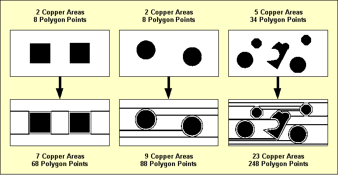
Figure 4-8: Automatic Copper Fill Complexity
You can use one of the
,
and
options instead of the
default option from the
function to reduce the complexity and number of fill areas. This allows for trace corners and/or full circles to be isolated like octagons, thus also reducing the amount of Gerber data if no Gerber arc commands can be used.
To avoid long response times after unintentionally activating the copper fill function, automatic copper fill can be canceled by pressing any key and confirming the abort request with a verification menu. Note, however, that canceling is not possible anymore at the final stage of connectivity generation, and that areas generated before the abort request must be explicitly eliminated using the
function.
Using the copper fill function considerably increases the number of copper areas and polygon points. This raises the CPU time requirements for the
function if the
function type is set to a corner to corner airline calculation (see
chapter 4.3.2 of this manual). In such cases it can be worthwhile to use a pin to pin calculation method to reduce
CPU time requirements. The
from the
Layout Editor
menu is used to set the
function type.
Copper Area Hatching
The
submenu provides the
function for transforming copper areas into line or cross hatched areas with user-definable hatching width and hatching clearance.
Hatching is accomplished through trace segments generation. The width of the produced trace segments can be set with the
function (default 0.3mm) whilst the spacing between produced trace segments can be set with the
function (default 1/20 inch).
The
function is used to designate the hatching type. The default
option generates hatch areas with diagonal trace segments. The
option generates hatch areas with crosswise intersecting diagonal trace segments.
The hatching process is activated by calling the
function and selecting the copper area to be hatched.
Use the following commands to set the coordinate display mode to inch, and transform the circle-shaped copper area on signal layer 2 of the layout to a line-hatched area with a hatching distance of 1mm:
| Settings | |
| Coordinate Display | |
| Display Inch | |
| Areas | |
| Copper Fill | |
| Hatching Distance | |
| Hatching Line Spacing ( 1.27mm) ? | 1 |
| Hatch Copper Area | |
| Move to Passive Copper Area/Signal Layer 2, [0.8",1.8"] | |
Use the following commands to set the hatching width to 0.2mm and transform the active copper area (signal
vdd) on signal layer 1 of the layout into a cross-hatched area:
| Areas | |
| Copper Fill | |
| Hatching Width | |
| Hatching Line Width ( 0.30mm) ? | 0.2 |
| Hatching Mode | |
| Grid Hatching | |
| Hatch Copper Area | |
| Move to Active Copper Area "vdd"/Signal Layer 1, [2.5",2.0"] | |
The
function generates a special layout polygon type called hatched copper area. The hatching and the hatching area outline are generated using traces with a trace width according to the hatching width setting. The traces are strongly connected with the hatched copper polygon to support general
Layout Editor polygon functions such as
or
.
The PCB layout example should now look like the one shown in
figure 4-9 if you correctly executed all operations.
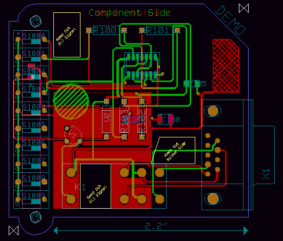
Figure 4-9: Layout with Filled Copper Areas
This might be a good time to save the layout:
| File | |
| Save Element | |
4.6.9 Library Update
The
function is one of the most powerful features of the
Bartels AutoEngineer.
is usually used to update a job-specific library in order to correlate it with the contents of some master library.
Use the following commands to copy the currently loaded layout to the
democopy.ddb DDB file (with default layout element name), and load the copied layout:
| File | |
| Save Element As | |
| File Name ? | democopy |
| Element Name ? | |
| Load Element | |
| Layout | |
| File Name ? | democopy |
| Element Name ? | |
Now the copied layout appears on the screen. However, this layout contains only those objects which are directly defined on the layout. The lower level library elements (parts, padstacks, pads) are not displayed since they have not been copied with the
function to prevent from overwriting existing library elements in the
democopy.ddb destination file. The system will issue either the
Connected pins missing!
message or the
Cannot load all elements (display not complete)!
message in the status line. Use the following commands to correlate the job-specific library of DDB file
democopy.ddb with the contents of DDB source file
demo.ddb:
| File | |
| Update Library | |
| Layout | |
| File Name ? | |
| Element Name ? | |
| Source File Name ? | demo |
After a few moments the system should issue a
Library elements replaced! message which means that all library elements referenced from the currently loaded layout have been copied from the specified library source file. Use the following commands to re-load the layout in order to display the library update
( works on DDB file level, it doesn't affect elements in main memory):
| File | |
| Load Element | |
| Layout | |
| File Name ? | |
| Element Name ? | |
The
function can also be used to correlate the job-specific library with the contents of a different layout library file. Use the following commands to perform a library update for the currently loaded layout using the library source file
demolib.ddb, and re-load the layout (note how the
r04a25 resistor package type is updated with the definition from
demolib.ddb):
| File | |
| Update Library | |
| Layout | |
| File Name ? | |
| Element Name ? | |
| Source File Name ? | demolib |
| Load Element | |
| Layout | |
| File Name ? | |
| Element Name ? | |
The
function is used for substituting selectable library elements with definitions from a certain library source file. Use the following commands to replace the
r04a25 part symbol and the
p1206 pad symbol of the current
democopy.ddb DDB file with the corresponding definitions from the
demo.ddb DDB file, and re-load the layout
( works on DDB file level, it doesn't affect elements in main memory):
| File | |
| Replace Element | |
| Part | |
| File Name ? | |
| Element Name ? | r04a25 |
| Source File Name ? | demo |
| Please confirm (Y/N) ? | y |
| Replace Element | |
| Pad | |
| File Name ? | |
| Element Name ? | p1206 |
| Source File Name ? | demo |
| Please confirm (Y/N) ? | y |
| Load Element | |
| Layout | |
| File Name ? | |
| Element Name ? | |
4.6.10 Back Net List
The
function from the
menu is most useful for certain applications such as high frequency design, where net list data is requested to be automatically generated from the copper located on the PCB.
The mode of operation of this function should be demonstrated using the currently loaded layout from DDB file
democopy.ddb. Delete the trace which connects the pins
NO1 and
4 of the parts named
K1 and
X1, and reset the definition of power layer
vss:
| Traces | |
| Delete Trace | |
| Move to Trace,e.g.[2.35",0.9"] | |
| Settings | |
| Set Power Layers | |
| 1: vss | |
| Net Name ? | - |
| End | |
Note how the deleted trace and power layer definition are replaced with airlines. Use the following commands to add a trace to connect the pins
2 and
1 of the parts named
R100 and
R101:
| Traces | |
| Add Trace | |
| Move to "R100.2",[1.4",2.4"] | |
| Move to "R101.1",[1.6",2.4"] | |
| Done | |
The system now indicates a short-circuit error. Use the following commands to save the layout, run
to generate a net list with the same file and element name, and immediately re-load the layout again
( stores to DDB file without changing the currently loaded net list data):
| File | |
| Save Element | |
| Utilities | |
| Back Netlist | |
| File Name ? | |
| Element Name ? | |
| File | |
| Load Element | |
| Layout | |
| File Name ? | |
| Element Name ? | |
Now the system performs a connectivity generation to correlate the layout with the net list which was previously generated with
. Note that there are no airlines displayed anymore after completing the connectivity generation. The layout does not contain any open connections and/or short-circuits anymore (you can check this with
and
from the
menu). Deleting the trace which was previously causing a short-circuit would now result in an airline display.
Another useful application of the
function net list generation from Gerber data which was previously loaded with the
CAM View module (for more details see
chapter 4.8 of this manual).
4.6.11 Blind and Buried Vias
Blind and buried vias are partial vias which can be used for layer changes when routing multilayer layouts. Routing with blind and buried vias can considerably increase the routability of multilayer layouts with four or more signal layers.
The BAE
Layout Editor features arbitrary pad layer assignment (see also
chapter 4.2.2 for more details on creating padstacks) and drill classes to support the definition of blind and buried vias. Drill classes should be assigned to certain layer-sets to support CAM drill data output for selectable layer-sets (see also
chapter 4.7 for more details on drill data output). There are no system-imposed restrictions on how to define and/or assign drill classes. You can, e.g., use drill class
A for layer-set 1-2, drill class
B for layer-set 2-3, drill class
C for layer-set 3-4, etc. Note, however, that the drill class assignment must be considered for correct drill data output by the
CAM Processor, and that the layout top layer setting (see also
chapter 4.3.1) gains special meaning when using blind and buried vias.
A typical configuration for 4-layer layouts is the definition of the vias
via (for all layers),
via_12 (for layer-set 1-2),
via_23 (for layer-set 2-3) and
via_34 (for layer-set 3-4). All these vias are simultaneously available for routing when selected to the via list (see also
chapter 4.3.4 for details on how to select vias)
The
Layout Editor command used during interactive routing automatically selects the via with the least possible layer occupancy. The same principle is applied by the
Autorouter. At least one via for all signal layers required for autorouting. Additionally, the
Autorouter can e.g., simultaneously use vias for the layer-sets 1-2-3, 1-2, 2-3, etc. However, to avoid backtracking ambiguities, the
Autorouter is restricted in that it can not use vias with multiple mutually intersecting layers. I.e., the
Autorouter refuses to use a via for layer-set 1-2-3 and another via for layer-set 2-3-4 at the same time (error message
Invalid via padstack (cannot use it)!).
Using the
CAM Processor for generating drill data output for the drill holes defined on partial vias requires corresponding drill class(es) to be specified.
The production of PCBs with blind and buried vias is usually more expensive than the production of standard multilayer boards. However, using blind and buried vias increases the routability of multilayer layouts and also supports advanced PCB manufacturing technologies such as plasma-etched via production processes.
4.6.12 Exiting the Layout System
Don't forget to save the currently edited layout element before exiting the
Layout Editor:
| File | |
| Save Element | |
Returning to Main Menu
The following commands can be used from each program module of the BAE layout system (except for the
Autorouter) to return to the BAE Main Menu (BAE Shell):
| File | |
| Main Menu | |
The
function automatically saves the currently loaded layout element. From the BAE Shell, the following command can be used to return to the operating system:
| Exit BAE | |
Exiting BAE
The following commands can be used from each program module of the BAE layout system to return to the operating system, i.e., to exit the
Bartels AutoEngineer:
| File | |
| Exit BAE | |
The
function activates a confirmation request if the currently loaded element has not yet been saved. In this case you should abort the
function, save the current element, and then call
again, as in:
| File | |
| Exit BAE | |
| Please confirm (Y/N) ? | n |
| File | |
| Save Element | |
| File | |
| Exit BAE | |
Special Layout Features
© 1985-2026 Oliver Bartels F+E • Updated: 11 October 2010, 10:30 [UTC]
|
