This chapter describes how to use the
Layout Editor, the
Autorouter, the
CAM Processor and
CAM View for creating layout library symbols and designing PCB layouts and for generating and processing CAM output and manufacturing data for the PCB production. The examples presented in this chapter introduce the concepts and advanced features of the BAE PCB design system in a logical sequence and will take the user from the creation of layout library symbols and the design and modification of a PCB layout through to the generation of manufacturing data for the PCB production. The PCB design example is based on the circuit drawing and net list data prepared in the preceding chapters and will be subject to further processing in the following chapter. The reader should work through this chapter without missing any sections to gain full understanding of the BAE PCB design system. Once a command has been used and/or explained, the operator is assumed to have understood its function and be able to perform it again. Subsequent instructions containing this command will be less verbose for easier reading and more speedy learning.
Contents
4.1 General
The
Bartels AutoEngineer PCB layout system essentially consists of an interactive
Layout Editor with integrated layout symbol editor and functions for automatic part placement and automatic copper fill, the
Bartels AutoEngineer for fully automated PCB routing, and
CAM Processor and
CAM View program modules for generating and processing CAM output and manufacturing data for PCB production. The following sections of this manual describe in detail how to use these modules.
4.1.1 Components and Features
Layout Editor
The floating point database used throughout the
BAE Layout Editor allows for the mixed specification of metric and imperial coordinate units. All placement coordinates including rotation angles can be specified with floating point values. There are no restrictions at the definition and placement of pads, copper areas, parts, traces, texts, etc. The user interface provides a genuine display even for the more complex structures such as circles or arcs. Area visibility can be defined according to mirror modes, thus supporting SMD pins with different pad shapes for component and solder side.
The Design Rule Check (DRC) operates in grid-free mode with a precision of eight digits behind the decimal point. The DRC provides constant monitoring of copper against net list, with visual indication of distance violations and short-circuits. The system supports both Online and Batch DRC. Online DRC performs incremental checks, i.e., only the modified items are checked real-time thus saving a lot of computation time.
The
facilities allow to use the
Layout Editor without fear of causing damage. Up to twenty commands can be reversed or undone by applying the
function and then reprocessed with the
function.
ensures data security and provides a powerful feature for estimating design alternatives.
Arbitrary parts of the layout can be selected to groups and then moved, rotated, mirrored, copied or saved (and subsequently used as templates).
Fast interactive part placement with instant connections update guarantees an optimum exploitation of the layout area. Part connections (unroutes, airlines) are dynamically calculated and instantly displayed during placement. Parts can be rotated at arbitrary angles, and they can be mirrored for SMT applications. Parts can be placed at arbitrary coordinates and polar coordinates are supported for placing parts on a circle. The part library supports part-specific preferences for part rotation and part mirroring. During manual placement, an alternate package type can be selected for the currently processed part.
The system supports genuine net-orientated Connectivity. This means that electrical connections can be realized through copper areas instead of traces connecting. Traces and copper areas can be created in grid-free mode with floating point precision. Highlight is used to indicate the selected and/or processed signal, and each point of the signal can be connected. The system also supports arc shaped traces as well as blind and buried vias with automatic via type selection.
The BAE layout system provides powerful automatic copper fill functions. Copper areas can optionally be generated with line or cross hatching. The BAE layout system also supports power layer definitions. Arbitrarily shaped active copper areas can be placed on power layers, thus featuring split power planes.
High frequency and analogous applications are supported by useful facilities for shrinking and/or enlarging copper areas at arbitrary expansion values. Trace segment lengths and copper area edge lengths can automatically be determined or measured for test or documentation purposes.
With the
Bartels User Language integrated to the
Layout Editor the user is able to implement enhanced CAD functions and macros, user-specific post processors, report and test functions, etc.
User Language programs can be called by applying the
function from the
menu or by pressing a key on the keyboard (hot key).
Autoplacement
The BAE layout system is equipped with powerful
Autoplacement functions.
Parts can be selected and/or deselected for automativ placement according to set principles either by specifying part names
(c1,
r2,
ic15, etc.) or by specifying library symbol names
(dil14,
so20,
plcc44, etc.), where wildcards are also permitted. The user can also select parts from certain blocks of a hierarchical circuit design. The functions for designating the parts to be placed are a useful feature for controlling the placement process in a way that e.g., first the plug(s) can be placed, then the DIL packages, then the capacitors, etc.
The matrix placement facilities are used for the automatic placement of selectable part sets to definable placement grids. Matrix placement is intended especially for the initial placement of homogeneous part types such as memory devices, block capacitors, test points, etc. Of course the matrix placement function also considers the default rotation angle and mirror mode settings.
Initial placement functions are provided for performing a complete placement by automatically placing not yet placed parts inside the board outline. The parts are placed onto the currently selected placement grid, where pre-placed parts such as plugs and LEDs are considered as well as the connectivity derived from the net list. The initial placement algorithm features automatic SMD and block capacitor recognition. The solder side can optionally be used for placing SMDs. Parts are automatically rotated in 90 degree steps, where part rotation can optionally be restricted to provide fault-robust insertion data. A part expansion parameter can be set to support automatic part spacing. The initial placement process is controlled by adjustable heuristic weight factors for evaluating part segment fitting and for considering different net list structures. Intermediate rip-up/retry passes are activated during initial placement to optimize board area exploitation.
The system also provides placement optimization functions for automatic part and pin/gate swap. The part swap facility mutually exchanges identical components at their insertion position to minimize unroutes lengths. The pin/gate swap facility analogously performs an iterative exchange of gates and/or pins and pin groups, where gates or groups can also be swapped between different parts. Fixed parts are excluded from placement optimization. The admissibility of pin/gate swaps is fairly controlled with appropriate library definitions. Either single pass or multi pass optimization can be applied, with the swap method (only part swap, only pin/gate swap or both part and pin/gate swap) to be selected as required. Applying placement optimization will usually cause a significant simplification of the routing problem, thus resulting in a considerable time saving at the subsequent Autorouting process.
Bartels Autorouter
The
Bartels Autorouter® is the culmination of years of research and practical routing experience. It has an impressive set of features and has the flexibility to route a wide range of PCB technologies, including analog, multilayer and SMT designs. The
Bartels Autorouter® has been incorporated in leading PCB layout systems throughout the world, setting new industrial standards of success, reliability and flexibility and dramatically reducing the requirement for manual routing in all boards. Its incorporation into other systems has varied considerably. With
Bartels AutoEngineer, all of the advanced features and capabilities of the
Bartels Autorouter® are available. With the
Bartels Autorouter®, an experienced BAE user should be able to complete the design of a eurocard PCB including schematic drawing and manufacturing data output in not more than one or two days.
Bartels Autorouter® is based on special backtracking/rip-up/reroute algorithms. These types of routing algorithms have been proven to be the only ones capable of achieving 100% route completion on the majority of today's challenging PCB designs. Extensive artificial intelligence features have been built into the router to produce high quality design results in a reasonable time. The
Bartels Autorouter® includes special features for production optimization giving excellent yield in board manufacture. The complete routing process is supervised by a backtracking algorithm, which not only prevents from a deterioration of the result or a dead-lock during rip-up or optimization but also is able to exploit a new and/or better routing solution.
Both the selective rip-up and the cross-net optimizer passes are assisted by a unique intelligent multi-net cleanup algorithm with pattern recognition. This algorithm identifies traces blocking unrouted connections and rips up and reroutes multiple connections or even trees at a time to improve the global routing result. The
Autorouter is capable of moving trace bunches to make space for not yet routed connections (push'n'shove routing). Cleanup passes for performing cross-net changes are applied during optimization and will considerably reduce via counts and straighten trace paths. All advanced routing features are supported by a sophisticated array of heuristic cost parameters which are dynamically adapted to produce quality routing results comparable to those made by skilled layout designers.
The
Bartels Autorouter® is capable of simultaneously routing up to 28 layers (16 signal layers and 12 power layers; multilayer routing).
The
Autorouter automatically identifies and connects pre-placed power supply structures thus ensuring correct power and ground routing. The router also utilizes automatic routines for correctly connecting SMD pins to power layers wherever necessary. This feature also supports any split power planes placed on the power layers (split power plane routing). Routing widths are pin-specific rather than net-specific. SMD pins are routed with the anticipated pin routing widths to avoid perpendicular positioning of SMD parts during the soldering process. T-shaped connections are automatically generated (full copper sharing).
The routing progress can be watched both graphically and on statistical readout on the
Autorouter user interface. The
Autorouter can be stopped at any time and then continued or re-started with changed parameters on demand.
Features are provided for automatically adapting layouts to placement and/or net list changes (re-entrant routing) where the
Autorouter evaluates pre-routed traces, identifies and removes wrong and redundant paths, and then routes open connections to achieve a correct 100% solution. Subsequently, the modified layout can be optimized again.
All of today's advanced PCB technologies are fully supported by the
Bartels Autorouter®. The
Autorouter is able to consider and/or connect arbitrarily shaped pads, traces, copper areas, power planes and keepout areas. The built-in off-grid recognition allows off-grid placement of parts and pre-routed traces. The
Autorouter supports standard routing grids with optional half-grid routing (1/20 inch to 1/100 and/or 1/200 inch), arbitrary routing grids for special pin pitches and grid-free routing. Multilayer SMD technologies are supported by the
Autorouter's SMD via preplace and BGA (Ball Grid Array) fanout routing algorithms, which can optionally be used if via pre-allocation is required for connecting SMD and/or BGA pins to inside layers with high priority. The
Bartels Autorouter® supports microvias (via-in-pad technology) and blind and buried vias with automatic via type selection thus increasing the routability of multilayer layouts and also supporting new PCB manufacturing technologies such as processes for producing plasma-etched vias. Area and block routing methods can be supported by defining keepout routing areas and/or prohibited layers, and the
Autorouter is capable of considering via keepout areas.
The
Autorouter provides the same initial placement and placement optimization functions as already known from the
Layout Editor, allowing for automatic pre-placement and placement optimization before starting the autorouting process.
The
Autorouter provides enhanced routing features such as placement optimization (pin/gate swap) during rip-up/retry routing, gridless routing, single net routing, component routing, area routing, mixed-grid routing, etc. The place and route function activates both the
(including complete initial placement and placement optimization) and the
(including complete
, rip-up/retry routing and optimizer), thus performing complete placement and routing on the push of a button. The single net routing function of the
Autorouter is used for automatically routing selectable nets and/or connections. The single net router can be applied to pre-rout power supply or critical nets with specific preferences for trace widths, clearance, layer assignments, etc. For completeness reasons the single net router also supports an option for selectively deleting already routed nets and/or connections. The
Autorouter provides a feature for selectively routing net groups (e.g., busses of a certain circuit block) using specific routing options for preferred routing directions, trace widths, etc. The component routing function can be used to rout selectable parts. The area/block routing function of the
Autorouter is used for routing selectable areas and/or circuit blocks. It is possible to define different routing areas according to circuit topology (I/O, memory, digital and/or analog part of the design, etc.) and perform autorouting using block-specific routing options such as routing grid, clearance, preferred routing direction, bus routing preferences, etc. During the rip-up autorouting process the
Autorouter utilizes features for automatically performing selective component and/or pin/gate swaps in cases where this might result in better routability of swapped parts, gates or pins.
The
facilities allow to use the
Autorouter without fear of causing damage. Up to twenty commands can be reversed or undone by applying the
function and then reprocessed with the
function. Since this is true even for most complex operations such as complete
Autorouter passes,
ensures data security and provides a powerful feature for estimating design alternatives.
With the
Bartels User Language integrated to the
Autorouter, the user is able to implement enhanced CAD functions and macros, user-specific placement and autorouting procedures, report and test functions, etc.
User Language programs can be called by applying the
function from the
menu or by pressing a key on the keyboard (hot key).
The
Autorouter module of the
BAE HighEnd system provides advanced autorouting technologies based on patented neural network technology
(Neural Autorouter). The
BAE HighEnd Autorouter supports skilled analog signal routing, automatic microwave structure generation, grid-less object-orientated routing with automatic placement optimization, etc. The
BAE HighEnd Autorouter also provides features for routing problem recognition and/or classification and for learning and automatically applying problem-adapted routing strategies and/or rules.
CAM Processor
The
Bartels AutoEngineer layout system allows for the definition and creation of arbitrarily shaped areas and pads which can also be rotated at any angle. All these features are supported by the intelligent
CAM Processor, which utilizes a series of automatic fill algorithms with multiple aperture selection and area reduction. I.e., pad definitions are not necessarily restricted to some particular tool set, but may fully support the demanded technology. The
CAM Processor automatically optimizes the use of the selected tools and aperture table definitions to generate all structures at highest possible precision with regard to the chosen plot parameters and output tolerance ranges. The system also provides appropriate error messages and highlight features to indicate objects which cannot be plotted using the selected tools and the current plot parameter settings. In-built functions are available for producing HP-GL pen plot, PCL laser print and Postscript output, and for supporting configurable drivers for Gerber photoplotting with freely definable aperture tables. The
CAM Processor also provides programming data for auto insertion and pick and place equipment, solder mask, drill data and SMD adhesive masks. CAM output is generated considering general parameters such as tool tolerance, scaling factor, CAM rotation and/or mirroring, freely definable CAM origin, etc. Special plot parameters for generating negative power layer and split power plane plots are also supported. With the flexibility of easily preparing all of the required output data the BAE user has free choice amongst photo plot producers and PCB manufacturers.
With the
Bartels User Language integrated to the
CAM Processor the user is able to implement enhanced CAM functions and macros, user-specific and/or batch-driven post processors, report and test functions, etc.
User Language provides unrestricted access to the BAE design database. The user is able to implement user-specific programs for exporting any data such as part lists, net lists, geometry data, drill data, insertion data, test data, milling data, etc. in freely definable formats.
User Language programs can be called by applying the
function from the
menu or by pressing a key on the keyboard (hot key).
CAM View
The
CAM View module provides features for displaying Gerber data, drilling data (Sieb&Meier and/or Excellon) and milling data (Excellon) in order to check CAM data validity and to estimate the efficiency of tool usage.
CAM View features multiple input and sorted output with variable offsets and adjustable aperture tables to support panelization.
CAM View also provides a powerful function for translating Gerber data to BAE layout design data, i.e., with
CAM View the user is able to import Gerber data produced by foreign PCB layout systems.
With
Bartels User Language integrated to the
CAM View module the user is able to implement enhanced
CAM View functions and macros, user-specific batch procedures, report and test functions, etc.
User Language programs can be called by applying the
function from the
menu or by pressing a key on the keyboard (hot key).
4.1.2 Starting the Layout System
It is recommended to start the
Bartels AutoEngineer from the directory where the design files should be generated since this considerably simplifies job file access. If you intend to process the examples provided with this manual it is recommended to move to the BAE examples directory installed with the BAE software. The
Layout Editor can be called from the
Bartels AutoEngineer main shell. Start the BAE shell by typing the following command to the operating system prompt:
> bae 
The
AutoEngineer comes up with the Bartels logo and the following menu (the
function is only available under Windows/Motif; the
and
menu items are available only with special software configurations such as
BAE HighEnd or
BAE IC Design):
Move the menu cursor to the
menu item and confirm this choice by pressing the left mouse button:
| Layout |  |
The
Layout Editor program module is loaded and the
Layout Editor menu is activated. Check your BAE software installation if this fails to happen (see the
Bartels AutoEngineer® Installation Guide for details on how to perform a correct installation).
It is also possible to call the
Layout Editor directly from the
Packager. In this case, layout element creation for the net list created by the
Packager is automatically suggested for designs not yet containing a corresponding layout.
4.1.3 Layout Editor Main Menu
The
Layout Editor standard/sidemenu user interface provides a menu area on the right side, consisting of the main menu on top and the currently active menu below that main menu. After entering the
Layout Editor the
menu is active and the menu cursor points to the
function.
The Windows and Motif versions of the
Layout Editor can optionally be operated with a pull-down menu user interface providing a horizontally arranged main menu bar on top. The
WINMENUMODE command of the
bsetup utility program is used to switch between
SIDEMENU and
PULLDOWN Windows/Motif menu configurations (see
chapter 7.2 for more details).
The following main menu is always available whilst processing layout elements with the
Layout Editor:
Undo, Redo
The functions provided with the
menu allow you to use the
Layout Editor without fear of causing damage. Up to twenty commands can be reversed or undone using
and then reprocessed with the
. This is true even for complex processing such as group functions or
User Language program execution.
ensures data security and provides a powerful feature for estimating design alternatives.
Display
The
or
menu can either be activated by selecting the corresponding main menu item or by pressing the middle mouse button. Activation through the middle mouse button is even possible whilst performing a graphical manipulation such as placing or moving an object. The
or
menu provides useful functions for changing display options such as zoom window, zoom scale, input and/or display grids, grid and/or angle lock, color settings, etc. The
or
menu also contains advanced display functions such as
and
.
Files
The
menu provides functions for creating, loading, saving, copying, replacing and deleting DDB elements. The
menu also allows to load and/or store color tables or to call important database management functions such as listing DDB file contents and performing library update.
Parts
The
provides functions for defining part placement groups, for manual part placement, for part renaming, for automatic part placement (matrix placement, initial placement) and for manual and automatic placement optimization (component swap, pin/gate swap). The function for selecting the via(s) for subsequent routing is also provided in this menu.
On part level, the
menu is used for placing, moving, deleting and renaming pins (i.e., padstack symbols). On padstack level, the
menu is used for placing, moving and deleting pads.
Traces
The
menu provides functions for interactive routing, i.e. for manually creating new traces and for modifying or deleting existing traces and/or trace segments.
Areas
The
menu is used for defining the board outline, for generating copper areas and power planes and for creating documentary lines and/or documentary areas. Existing areas can be moved, rotated, mirrored, copied and deleted.
The
menu also provides the copper fill functions for defining copper fill workareas, for automatic copper fill area generation and/or elimination and for hatched copper area creation.
Text, Drill
The
menu is used for creating, moving, changing and deleting texts on any layout hierarchy level. On padstack level, the
menu provides additional functions for defining drill holes.
Groups
The
menu provides functions for selecting elements to group, for moving, rotating, mirroring, scaling, copying, deleting, fixing, releasing, saving and loading groups, and for replacing symbols in a group.
Parameter
The
menu provides functions for selecting the layout library, setting the origin and the element boundaries of the currently loaded element, defining power layers, selecting the mincon function for the airline display, setting the spacing design rule parameters and activating the automatic design data backup feature.
Utilities
The
menu provides functions for exiting BAE, returning to the BAE main shell, calling the
Autorouter or the
CAM Processor, starting the batch design rule check, generating net list data from current copper
(), defining area mirror visibility and starting
User Language programs.
4.1.4 Customized Layout Editor User Interface
Menu Assignments and Key Bindings
The BAE software comes with
User Language programs for activating a modified
Layout Editor user interface with many additional functions (startups, toolbars, menu assignments, key bindings, etc.). The
bae_st User Language program is automatically started when entering the
Layout Editor.
bae_st calls the
uifsetup User Language program which activates predefined
Layout Editor menu assignments and key bindings. Menu assignments and key bindings can be changed by modifiying and re-compiling the
uifsetup source code. The
hlpkeys User Language program is used to list the current key bindings. With the predefined menu assignments of
uifsetup activated,
hlpkeys can be called from the
function of the
menu. Menu assignments and key bindings can be listed with the
uifdump User Language program. The
uifreset User Language program can be used to reset all currently defined menu assignments and key bindings.
uifsetup,
uifdump and
uifreset can also be called from the menu of the
keyprog User Language program which provides additional facilities for online key programming and
User Language program help info management.
Context-sensitive Function Menus
Pressing the left mouse button in the graphic workarea activates a context-sensitive menu with specific functions for the object at the current mouse position if no other menu function is currently active. The
and/or
file management functions are provided if no element is currently loaded. This feature is implemented through an automated call to the
ged_ms User Language program.
Cascading Windows/Motif Pulldown Menus
The Windows and Motif pulldown menu user interfaces of the
Layout Editor provide facilities for cascading submenu definitions. I.e., submenus can be attached to other menu items. The
uifsetup User Language program configures cascading submenus for the pulldown menu interfaces of the Windows/Motif
Layout Editor modules. This allows for easy submenu function location (and activation) without having to activate (and probably cancel) submenus. The function repeat facility provided through the right mouse button supports cascading menus to simplify repeated submenu function calls.
Windows/Motif Parameter Setup Dialogs
The following Windows/Motif parameter setup dialogs are implemented for the
Layout Editor:
- - : General Layout Editor Parameters
- - : Display Parameters
- - - : Automatic Placement Parameters
- - - : Copper Fill Parameters
The
uifsetup User Language program replaces the parameter setup functions of the Windows and Motif pulldown menus with the above menu functions for activating the corresponding parameter setup dialogs.
Windows/Motif Pulldown Menu Konfiguration
When using pulldown menus under Windows and Motif, the
uifsetup User Language program configures the following modified
Layout Editor main menu with a series of additional functions and features:
4.1.5 In-built Layout System Features
Automatic Parameter Backup
The
Layout Editor provides an in-built feature for automatically saving important design and operational parameters with the currently processed SCM sheet and/or SCM library hierarchy level. The following parameters are stored to the current design file when activating the
function:
- Autosave Time Interval
- Name of the currently loaded Layout Color Table
- Input Grid
- Display Grid
- Grid/Angle Lock
- Coordinate Display Mode
- Wide Line Draw Start Width
- Group Display Mode
- Part Placement Default Rotation Angle
- Part Placement Default Mirror Mode
- Default Text Size
- Part Airline Display Mode
- Standard Trace Widths
- Trace Segment Move Mode
- Library File Name
- Mincon Function Type
- Placement Matrix
- Placement Matrix Enabled Flag
- Copper Fill Isolation Distance
- Copper Fill Minimum Area Structure Size
- Copper Fill Trace Cutout Mode
- Copper Fill Island Delete Mode
- Copper Fill Heat Trap Mode
- Copper Fill Heat Trap Width
- Hatching Line Spacing
- Hatching Line Width
- Hatching Mode
Parameter sets are stored with special names according to the currently processed layout database hierarchy level. The layout element name is used for layout elements, parameter set name
[part] is used for layout part symbol elements,
[padstack] is used for layout padstack elements and
[pad] is used for layout pad elements. When loading an element, the corresponding parameter set is automatically loaded and/or activated as well, thus providing a convenient way of activating a default parameter set suitable for processing the selected design and/or library element type.
Layer Assignments
The layer assignment is most important for the creation and modification of layout symbols and for the design of layouts. The system provides the following layers and/or display items:
- Signal Layers 1 - 100
- Signal Layer "Top Layer"
- Signal Layer "All Layers"
- Signal Layer "Middle Layer"
- Power Layers 1 - 12
- Documentary Layers 1 - 100
- Board Outline
- Airlines
- Drill Holes
- Workarea
- Origin
- Errors
- Highlight
- Drill "-", "A" - "Z"
- Fixed
- Glued
The signal layers are subject to the design rule check. On the signal layers the electrical conductivity of the PCB is defined by creating and/or placing traces, pads and passive or active copper areas.
,
and
are special signal layers.
The
can be dynamically assigned to a certain signal layer during the layout design process. On default, the
is assigned to signal layer 2. The
is most useful when generating library symbols for multilayer designs with an arbitrary number of layers. The
function from the
menu is used to assign the PCB top layer, thus defining the number of PCB layers. The mirror functions (e.g., for mirroring parts) will always consider the current top layer setting, i.e., signal layers beyond the top layer are not affected by mirror functions.
Note that the menu item text for selecting the
can be changed with the BAE setup to provide a user-specific menu text such as
or
. See the description of the
bsetup utility program for more details on customizing the layout signal layer menus.
The
signal layer includes all signal layers from signal layer 1 (solder side) to the currently defined top signal layer (component side). Objects defined on
are considered to be placed on all signal layers and are checked and plotted accordingly. The
signal layer is most useful for the definition of library symbols such as drilled pins with identical pad shapes on all signal layers.
The
signal layer matches all signal inside layers, i.e., the
signal layer includes all layers between signal layer 1 (solder side) and the currently defined top signal layer (component side). Objects defined on
are considered to be placed on all signal inside layers and are checked and plotted accordingly. The
signal layer considerably simplifies pin definitions for multilayer layouts where inside layer pad shapes differ from component and solder side pad shapes.
Up to twelve power layers can be defined with each layout, all of which being negatively displayed and plotted by the system. The
function from the
menu is used to assign power layer signal names such as
gnd,
0v or
vcc to define the power layers of the currently loaded layout. The
Layout Editor allows for the DRC-controlled definition of split power planes by (hierarchically) placing active copper on power layers. The
CAM Processor automatically generates isolations and heat traps when plotting power layers.
The documentary layers are used to store and/or include documentary information (graphic, text) and special keepout definitions with the layout and/or the layout library symbols. The
bsetup utility program can be used to define up to 100 different (or 12 in
BAE Professional simultaneously accessible) documentary layers with individual names and characteristics according to special requirements. The system allows for the definition of customer-specific documentary layers for, e.g., silk screen, insertion data, solder resist, glue spots, drill plan and drill overlap control, plot markers, part spacing check, comments, measuring, etc. Each documentary layer consists of the following sides to support double-sided SMD design:
Each documentary layer side is a sub-layer of the corresponding documentary layer. The
and
sub-layers are mutually interchanged when performing mirroring. The
CAM Processor can optionally plot the
sub-layer together with
and/or
. Documentary layer definitions have fundamental influence on what can be defined in the layout and which CAM output can be produced. Documentary layer definition changes introduced by
bsetup only apply to subsequently defined library symbols to enable data exchange between different configurations. It is strongly recommended to become familiar with the features for defining documentary layers (and to define documentary layers according to your specific requirements) before starting with the design of real layouts or layout symbols for productive use. See
chapter 7.2 of this manual for a description of the
bsetup utility program and for the default documentary layer definitions provided with initial BAE software installations.
The
layer is used for defining and/or displaying the board outline of the currently loaded layout. The
layer is used for displaying unroutes on the currently loaded layout. The
layer is used for displaying drill holes on the currently loaded layout, part or padstack.
,
,
and
are layers for displaying special layout user interface elements.
The layers are used for assigning colors to drill classes. The and layers are used for the selection of patterns for the display of fixed and/or glued layout elements.
Pick Preference Layer and Element Selection
The pick preference layer is used to resolve ambiguities when selecting objects which are placed at the same position but on different layers (e.g., traces, areas, SMD parts, etc.). The pick functions use the pick preference layer to designate the element to be selected, if more than one object of interest is placed at the pick position. The pick preference layer can be selected with the
function from the
menu. On default, the pick preference layer is set to signal layer 1 (solder side).
The
dialog from the
menu provides the
parameter for selecting the element pick method for multiple elements at the same pick position. The
default option picks an element from the currently selected preference layer. The
option provides an element selection facility if more than one element is found at the pick position. A loop for highlighting the selectable elements with status line short description is activated. The highlighted element can be selected through return key or left mouse button click. This element selection can be aborted through escape key or right mouse button input. Any other key switches to the next element at the pick position.
Net List
A net list is usually required for the layout design. In BAE, the net list is commonly created with the
Schematic Editor and will then be transferred to the layout using the
Packager. Alternatively, ASCII net lists can be imported to the BAE layout system using utility programs such as
conconv or
redasc. See
chapter 3.4 of this manual for more details on net list processing.
The function for loading a layout will not only load the pertinent data from the lower hierarchy levels (parts, padstacks and pads), but also the corresponding net list. The net list data is correlated with all geometrical data on the layout ("Connectivity Generation"). Please note that the element names for both the layout and the net list must be identical for this to work.
After successfully generating the connectivity, the system is capable of instantly controlling and/or correlating each layout modification with the net list definitions. This high-sophisticated layout design feature is called "Full Copper Sharing" or "True Connectivity". Full copper sharing enables real-time recognition of electrical connections, no matter whether connections are created with traces, copper areas or vias. I.e., the system supports advanced routing features such as cross connection recognition, genuine T-connections, lining up traces created with group copying, implementing routes with arbitrarily shaped copper areas, etc.
The
BAE HighEnd layout connectivity evaluation system uses special data structures for storing additional information about the structure of electric connections between copper elements. This requires more memory compared to
BAE Professional, but results in dramatically shortened response times when manually editing large nets or moving parts since only the elements in the neighborhood of the currently processed object have to be considered by the DRC.
Mincon Function
Not yet routed connections (unroutes) are displayed as airlines. During part placement, the
function performs dynamic (real-time) recalculation of these airlines in order to display minimum length airline sets. This makes the
function an indispensable utility for achieving an optimum placement. The
menu item from the
menu is used to set the type of airline display, i.e., to choose the method of calculating unroutes from pin-to-pin or corner-to-corner minimization where also the unroute components to be calculated can be selected (horizontal only, vertical only, horizontal + vertical sum, etc.).
BAE HighEnd utilizes modified data structures for internal connectivity representation and airline calculations. The
BAE HighEnd
functions run at much higher performance compared to
BAE Professional, however, at the cost of higher memory requirements.
Design Rule Check
The BAE design rule check utilizes full copper sharing features to perform real-time recognition of open connections, short-circuits and distance violations. Open connections (unroutes) are displayed as airlines, short-circuits are indicated with highlight, and distance violations are enclosed by a rectangle. The corresponding colors for displaying
,
and
can be selected with the
function from the
menu.
Only modified items are checked real-time by the incremental online design rule check, thus saving a lot of computing time. As board parameters could have changed until post-processing, it is recommended to use the
function from the
menu for a final batch design rule check with the current layout parameter settings before releasing the board. The incremental connectivity, however, does not have parameters and thus is always correct. The
function from the
menu should be used after
to check all error counts.
The spacing parameters for the distance checks can either be set from the
menu (functions
,
and
) or can be defined as net-specific parameters in the net list using the
MINDIST net attribute). Note, however, that these parameter settings need not be the same as for the autorouting since the
Autorouter can automatically set minimum distance parameters according to the routing grid selection. Net-specific spacing parameters are individually considered by the
Autorouter.
Groups
The
Layout Editor group functions provide powerful features for design data manipulation. An arbitrary set of items of the currently loaded layout or part can be selected to a group which then can then be saved, moved, rotated, mirrored, scaled, copied, deleted, fixed or unfixed.
The group functions are featuring set principles. Elements can be added (selected) to or removed (deselected) from the currently defined group. Highlight display is used to indicate group-selected items. The
function is used to select and/or deselect parts, traces, areas, texts, visible and/or invisible elements or elements of any type by defining an area around the items to be selected. The
function is used to select and/or deselect single elements of a certain type (part, trace, area or text) by picking the desired items. The
function is active as long as valid pick elements are selected, thus allowing for the selection of a series of objects of a certain type). The
function is used to deselect all items from the current group.
All group-selected elements are subject to subsequent group functions such as
,
,
and
. The
and
functions only work on group-selected parts, traces and vias.
The number of modified elements is displayed with the feedback messages of
,
,
,
and
functions. This information can be used to check whether the group function was applied as intended.
The
function is used to save the currently defined group. The
function prompts for a group origin selection which becomes the origin of the new element> The group origin is also used as the reference point for group load commands. Saved groups are stored as an element of the same type as that from which the group was selected. To prevent from unintentionally overwriting existing database elements,
prompts for confirmation if the specified element already exists in the destination file. The
function can be used to reload previously saved groups (as well as layout and/or part elements) to different layouts and/or parts. The save and load group facilities can be used for a variety of tasks such as replicating tracking, saving and loading PCB templates, stealing from existing and proven designs, etc.
The
and
functions do not perform automatic part and/or pin renaming when copying and/or loading groups including parts (on layout level) or padstacks (on part level). Naming conflicts are resolved by assigning
# names to parts and/or pins, and manual renaming is required to correct the name list (or some special
User Language program must be implemented for solving such name list problems automatically).
Pressing the right mouse button during group movement operations such as
,
or
activates a submenu with functions for placing the group to relative or absolute coordinates
(,
), rotating the group
(,
,
), mirroring the group (around the X-axis using either
and/or
) or even scaling the group element dimensions and placement coordinates
(, applied after placing the currently processed group). The
submenu provides the
option for automatically rerouting traces between the moved group and the rest of the layout after selecting the start point for the group move operation.
first expects an interactive selection of a quadrant origin and then prompts for the quadrant (Upper Right, Upper Left, Lower Left, Lower Right). Subsequent group move operations are only applied on group-selected elements and/or points placed within the selected quadrant. It is possible to move parts of a layout and to reroute the connections to the moved group. Note, however, that the algorithm applied by the group move functions for rearranging traces is not a genuine routing algorithm and is designed to be applied on horizontal and/or vertical move operations only. For more complex group shift operations it is recommended to discard the routing and perform a re-routing using the appropriate
Autorouter procedures.
The
function first resets the currently defined group to deselect all group elements before performing the load operation. After successfully loading a group, all loaded group elements are automatically group-selected. I.e., only loaded group elements are subject to subsequent group functions.
The
Layout Editor supports different options for displaying group-selected elements during group movement operations. The behavior of this feature can be controlled with the
function which provides the following display modes:
| Groups | |
| Display Mode | |
deactivates the group movement display.
displays upper level group-selected elements which are assigned to the group display layer; the group display layer is a BAE setup parameter defined with the
LAYGRPDISPLAY command of the
bsetup utility program (see
chapter 7.2 for a description of
bsetup).
displays all group-selected elements except for traces, vias and drill holes during group movement.
displays all group-selected elements including traces, vias and drill holes during group movement.
is the default setting.
The
function is used to replace group-selected part macros (on layout level) or padstack macros (on part level). This function is most useful for fast pin type replacement (technology change) on part level.
On layout level, the
function supports alternate part package type assignments for net list parts which include the specified part macro in their alternate part package type list. Package types for non-netlist parts, however, are changed without this check.
Fixing/Releasing Elements
Certain layout elements such as parts or traces can be fixed. Fixed objects are not changed by subsequent automatic processes such as placement optimization, automatic pin/gate swap or autorouting. It is strongly recommended to fix critical elements such as parts (e.g., plugs, switches, LEDs, etc.) which are to be excluded from the placement optimization or manually pre-routed traces (e.g., for power supply) which must not be changed by the
Autorouter. A specific highlight for indicating fixed elements is activated during fix and release operations.
All functions for manipulating and/or copying fixed elements (parts, traces, vias) preserve and/or copy existing fixed modes. This also means that the
Layout Editor trace functions for interactive routing keep traces fixed flags when processing pre-routed fixed traces. I.e., when manipulating pre-routed fixed traces, there is no need of re-fixing such traces to prevent the
Autorouter from re-routing and/or rejecting pre-routed traces.
Polygons, Areas
In the Layout Editor, the functions from the
menu are used to create and/or modify polygons and/or pad shapes. Each polygon definition is associated with a layer and/or a polygon type and can contain an arbitrary number of arcs. The definition of an arc is applied by selecting either the
or the
option from the submenu to be activated after specifying the arc start point; subsequently, the system expects the arc center point specification, and the arc definition is completed with the arc end point selection. The system provides instant display of the resulting circle and/or arc during interactive input of the arc center and end points. At the definition of full circles, the input of the arc end point is superfluous, i.e., the full circle definition can be completed with the
submenu function to be activated after setting the arc center point.
The algorithm for picking polygon corners and polygon segments picks the polygon element with minimum distance from the pick point if more than one possible pick element is within snapping distance. This allows for reliable selection of polygon elements even when working in (small) zoom overview display modes.
Project and Version Control Attributes
The
$pltfname (element file path name),
$pltfsname (element file name) and
$pltename (element name) texts can be placed to display the project file path name, the project file name (without directory path) and the element name of the currently loaded element.
The
$plttime (current time),
$pltdatede (current date, German notation) and
$pltdateus (current date, US notation) system attributes are substituted with the current time and/or date when displayed and/or plotted on layout level.
The
$pltstime (save time),
$pltsdatede (save date, German notation) and
$pltsdateus (save date, US notation) system attributes are substituted with the time and date at which the currently loaded layout was last saved.
Automatic time and date substitutions are applied throughout all database hierarchy levels (pad, padstack, part, layout), unless other attribute values are explicitly set for these attributes.
Measuring
The
Layout Editor automatically activates a measuring function when placing new text with the hash character as text string
(#). This measuring function determines the distance between the two input coordinates subsequently to be specified. The resulting text string is built from the corresponding distance value with length units (inch or mm) retrieved from the current coordinate display mode as selected with the
function from the
menu.
Considering CAM Output Restrictions
The
Layout Editor supports the definition of arbitrarily shaped areas and pads which can also be rotated at any angle. All these features are supported by the intelligent
CAM Processor, which utilizes a series of automatic fill algorithms with multiple aperture selection and area reduction. The
CAM Processor automatically optimizes the use of the selected tools and aperture table definitions in order to generate all structures at highest possible precision with regard to the chosen plot parameters and output tolerance ranges. The system also provides appropriate error messages and highlight to indicate objects which cannot be plotted using the selected tools and the current plot parameter settings.
As mentioned above, the
CAM Processor is able to construct arbitrary polygons. When defining pads, consideration should, however, be given to the way in which Gerber photo plot data is generated. A flash code containing only one set of coordinates is used for areas that match apertures such as circles and squares. For areas that don't match apertures efficient drawing techniques generating few coordinates are used where possible (e.g., with rectangles), but with some shapes and sizes much more coordinates are needed. With careful design of pads and appropriate aperture tables and plot parameter settings, much smaller Gerber data files can be generated, making them quicker to copy, cheaper to send by modem, less expensive to plot and require less media space, thus considerably reducing the costs incurred by the CAM and manufacturing process.
User Language
The
Bartels User Language Interpreter is integrated to the
Layout Editor, i.e.,
User Language programs can be called from the
Layout Editor, and it is possible to implement any user-specific
Layout Editor function required such as status display, parameter setup, reports and test functions, CAD/CAM input/output functions, symbol library management utilities, automatic or semi-automatic placement and/or routing functions, customer-specific batch procedures, etc.
The
Layout Editor provides both explicit and implicit
User Language program call facilities.
User Language programs can be started with explicit program name specification using the
function from the
menu (empty string or question-mark
(?) input to the program name query activates a
User Language program selection menu).
User Language programs can also be called by simply pressing special keys of the keyboard. This method of implicit
User Language program call is supported at any time unless another interactive keyboard input request is currently pending. The name of the
User Language program to be called is automatically derived from the pressed key, i.e. pressing a standard and/or function key triggers the activation of a
User Language program with a corresponding name such as
ged_1 for digit key
1,
ged_r for standard key
r,
ged_# for standard key
#,
ged_f1 for function key
F1,
ged_f2 for function key
F2, etc.
The Layout Editor
User Language Interpreter environment also features event-driven
User Language program calls, where
User Language programs with predefined names are automatically started at certain events and/or operations such as
ged_st at
Layout Editor module startup,
ged_load after loading a design element,
ged_save before saving a design element,
ged_tool when selecting a toolbar item and
ged_zoom when changing the zoom factor. The module startup
User Language program call method is most useful for automatic system parameter setup as well as for key programming and menu assignments. The element save and load program call methods can be used to save and restore element-specific parameters such as the zoom area, color setup, etc. The toolbar selection event must be used to start
User Language programs which are linked to toolbar elements. The zoom event can be used to apply an update request to a design view management feature.
Bartels User Language also provides system functions for performing key programming, changing menu assignments and defining toolbars. These powerful features can be applied for user interface modifications. Please note that a large number of additional functions included with the
Layout Editor menu are implemented through the
User Language programs delivered with the BAE software.
See the
Bartels User Language Programmer's Guide for a detailed description of the
Bartels User Language (chapter 4.2 lists all
User Language programs provided with the BAE software).
Neural Rule System
A series of advanced
Bartels AutoEngineer features are implemented through the integrated
Neural Rule System. See
chapter 6.3.2 for the rule system applications provided with the PCB layout system.
4.2 Layout Library Symbol Design
The
Bartels AutoEngineer is shipped with an extensive layout library. Nevertheless, you might require a certain layout symbol which has not yet been defined in these libraries. This section shows in detail how to create layout library symbols. The example symbols are created starting with the lowest DDB hierarchy level. I.e., first of all some pad and padstack symbols are defined, and, subsequently, some layout part symbols are defined. All these symbols will be stored to a DDB file named
demo.ddb. Use the following commands to move to the BAE examples directory (e.g.,
c:\baejobs) and start the
Bartels AutoEngineer:
>  C:
>  cd c:\baejobs
>  bae
The BAE main menu is activated, and you can start the
Layout Editor with the following command:
| Layout | |
The
Layout Editor is activated, and you can create layout library elements. You should become familiar with the conventions used for layout symbol design before generating your own symbols. Technology-dependent and manufacturing-specific conventions are usually to be considered with regard to pad shape definitions, part insertion pick points, identification of part pin
1, pin placement grids, part placement origin, minimum text sizes, drill symbols, part spacing parameters for SMDs, etc. The layer assignment is most important for the creation and modification of layout symbols and for the design of layouts in order to provide correct and complete CAM data output later (see
chapter 4.1.5 for more details).
Figure 4-1 shows the layout library symbols to be created in the following sections.
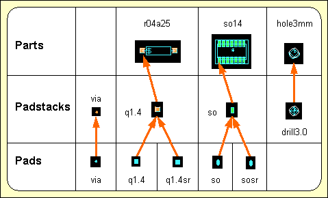
Figure 4-1: Layout Library Symbols
4.2.1 Creating Layout Pads
On layout pad level the pad shapes (i.e., the pin contact areas) are defined by creating passive copper areas. Different pad symbols can be assigned to different layers on a single padstack symbol thus defining a particular layout pin type.
It is recommended to refrain from assigning layers to the copper areas created on pad level, i.e., layer assignment should be disabled on pad level (this is the default setting introduced by
bsetup). The layer assignment can later be applied on padstack level to minimize the expenditure for adapting layout libraries to different manufacturing technologies.
Creating a Pad Symbol
Use the following commands to create a new pad symbol named
via with an element size of 1*1mm in DDB file
demo.ddb:
| File | |
| New | |
| Pad | |
| File Name ? | demo |
| Element Name ? | via |
| Element Width (mm/") ? | 1 |
| Element Height (mm/") ? | 1 |
The display now shows a square frame with a cross in the middle. The frame describes the element boundaries of the pad, and the cross marks the position of the element origin.
Defining a Copper Area
Use the following commands to define a circle-shaped copper area with a diameter of 0.9mm on the currently loaded pad element:
| Areas | |
| Add Passive Copper | |
| Jump Absolute | |
| Absolute X Coordinate (mm/") ? | 0.45 |
| Absolute Y Coordinate (mm/") ? | 0 |
| Arc Left | |
| Jump Absolute | |
| Absolute X Coordinate (mm/") ? | 0 |
| Absolute Y Coordinate (mm/") ? | 0 |
| Done | |
Setting the Element Boundaries
The pad symbol's element boundaries should be reduced to enclose the pad definition as densely as possible. This is accomplished with the following commands:
| Settings | |
| Upper/Right Border | |
| Absolute X Coordinate (mm/") ? | 0 |
| Absolute Y Coordinate (mm/") ? | 0 |
| Lower/Left Border | |
| Absolute X Coordinate (mm/") ? | 0 |
| Absolute Y Coordinate (mm/") ? | 0 |
Saving the Element
You can also place documentary information such as text, documentary lines or documentary areas on pad level. However it is recommended to refrain from placing documentary items on pad level since this would result in a very specific pad definition which could be used in quite few superior layout symbols. Use the following commands to save the pad symbol:
| File | |
| Save Element | |
Now the new pad symbol named
via is completely defined and stored to the DDB file
demo.ddb. This pad will later be loaded to a padstack thus defining a via for manual and automatic routing.
Defining Square Pads
Use the following commands to define a pad named
q1.4 with a square-shaped copper area (edge length 1.4mm) in DDB file
demo.ddb:
| File | |
| New | |
| Pad | |
| File Name ? | demo |
| Element Name ? | q1.4 |
| Element Width (mm/") ? | 2 |
| Element Height (mm/") ? | 2 |
| Areas | |
| Add Passive Copper | |
| Jump Absolute | |
| Absolute X Coordinate (mm/") ? | 0.7 |
| Absolute Y Coordinate (mm/") ? | 0.7 |
| Jump Relative | |
| Relative X Coordinate (mm/") ? | -1.4 |
| Relative Y Coordinate (mm/") ? | 0 |
| Jump Relative | |
| Relative X Coordinate (mm/") ? | 0 |
| Relative Y Coordinate (mm/") ? | -1.4 |
| Jump Relative | |
| Relative X Coordinate (mm/") ? | 1.4 |
| Relative Y Coordinate (mm/") ? | 0 |
| Done | |
| File | |
| Save Element | |
With the commands above, a pad named
q1.4 has been defined which will be used on a padstack for parts with plated-through pins. This pin definition will require a corresponding pad symbol for the solder resist mask, which should be same as
q1.4 except for a slightly expanded copper area. Use the following commands to copy the (still loaded) pad named
q1.4 to a pad symbol named
q1.4sr (square 1.4mm, solder resist), then load pad
q1.4sr and enlarge the copper area of
q1.4sr by 0.1mm:
| File | |
| Save Element As | |
| File Name ? | |
| Element Name ? | q1.4sr |
| Load Element | |
| Pad | |
| File Name ? | |
| Element Name ? | q1.4sr |
| Areas | |
| Resize Area | |
| Move to Area Corner/Edge | |
| Expansion Distance (mm/") ? | 0.1 |
| File | |
| Save Element | |
Defining Finger Pads
Use the following commands to define a pad named
so with a finger-shaped copper area (width 0.7mm, length 1.7mm) in the
demo.ddb DDB file:
| File | |
| New | |
| Pad | |
| File Name ? | demo |
| Element Name ? | so |
| Element Width (mm/") ? | 1 |
| Element Height (mm/") ? | 2 |
| Areas | |
| Add Passive Copper | |
| Jump Absolute | |
| Absolute X Coordinate (mm/") ? | 0.35 |
| Absolute Y Coordinate (mm/") ? | 0.5 |
| Arc Left | |
| Jump Relative | |
| Relative X Coordinate (mm/") ? | -0.35 |
| Relative Y Coordinate (mm/") ? | 0 |
| Jump Relative | |
| Relative X Coordinate (mm/") ? | -0.35 |
| Relative Y Coordinate (mm/") ? | 0 |
| Jump Relative | |
| Relative X Coordinate (mm/") ? | 0 |
| Relative Y Coordinate (mm/") ? | -1 |
| Arc Left | |
| Jump Relative | |
| Relative X Coordinate (mm/") ? | 0.35 |
| Relative Y Coordinate (mm/") ? | 0 |
| Jump Relative | |
| Relative X Coordinate (mm/") ? | 0.35 |
| Relative Y Coordinate (mm/") ? | 0 |
| Done | |
| File | |
| Save Element | |
With the commands above, a pad named
so has been defined which will be used to define a standard SMD pin for SO (small outline) package types. Use the following commands to copy the (still loaded) pad named
so to a pad symbol named
sosr (small outline pad, solder resist), load the
sosr pad and enlarge the copper area of
sosr by 0.05mm:
| File | |
| Save Element As | |
| File Name ? | |
| Element Name ? | sosr |
| Load Element | |
| Pad | |
| File Name ? | |
| Element Name ? | sosr |
| Areas | |
| Resize Area | |
| Move to Area Corner/Edge | |
| Expansion Distance (mm/") ? | 0.05 |
| File | |
| Save Element | |
Checking the File Contents
Within this section we have created a series of pad symbols which we stored to DDB file
demo.ddb. Use the following commands to list the pad(s) defined in the
demo.ddb DDB file:
| File | |
| File Contents | |
| Pad | |
| File Name ? | |
An empty string input (i.e., pressing the return key
) to the file name prompt causes the system to use the file name of the currently loaded element, which in our example is
demo.ddb. The system now produces the following listing of the pads contained in
demo.ddb:
Type : Pad / File : demo.ddb


: q1.4           : q1.4sr         : so              : sosr
: via            - End -
Hit the spacebar to continue.
4.2.2 Creating Layout Padstacks
On layout padstack level the layout pin symbols and vias are defined by placing symbols from the subordinate pad level. Each pad can be assigned to a signal and/or documentary layer thus designating contact areas for the routing or defining pad shapes for solder resist, SMD masks, etc. A drill hole and drill plan info can be created optionally for the definition of vias or drilled pins. Keepout areas can be utilized for controlling the pin contact mode. Documentary lines or areas can serve as pin designators on the silk screen or insertion plan, and reference texts can be used for displaying pin names on part and/or layout level.
In this section the pad symbols defined in the previous section are used to generate some padstack symbols. To provide visual input control it is recommended to use the following commands to change the color setup in order to display the
as well as the
() and the
(all sides) documentary layers during padstack definition:
| Change Colors | |
| Drill Holes | |
| Move to Desired Color, white | |
| -> Doc.-Layer | |
| Drill Plan/Both Sides | |
| Move to Desired Color, light blue | |
| Solder Mask/Both Sides | |
| Move to Desired Color, gray | |
| Solder Mask/Side 1 | |
| Move to Desired Color, dark gray | |
| Solder Mask/Side 2 | |
| Move to Desired Color, light gray | |
| Exit | |
Changing some item-specific color is accomplished by selecting the desired display item using the left mouse button and then selecting the desired color button from the
function from the
menu. In the layout system, the
menu provides a feature for fast display item fade-out/fade-in. Activating and/or deactivating some item-specific display is accomplished by selecting the desired display item entry with the right mouse button which works as a toggle between fade-out and fade-in. The system won't loose information on currently defined colors of faded-out display items; strike-through color buttons are used for notifying currently faded-out display items.
Use the following commands to store the currently defined color table with name
stackedit to the
ged.dat system file (in the BAE programs directory):
| View | |
| Save Colors | |
| Element Name ? | stackedit |
Once a color table has been saved it can be reloaded at any time using the
function from the
menu. Special color tables (e.g., for library edit, for finding unroutes, etc.) can be defined and reloaded on request. The default color table to be loaded after startup is the one named
standard.
Creating a Padstack Symbol
Use the following commands to create a padstack symbol named
via with an element size of 1*1mm in DDB file
demo.ddb:
| File | |
| New | |
| Padstack | |
| File Name ? | demo |
| Element Name ? | via |
| Element Width (mm/") ? | 1 |
| Element Height (mm/") ? | 1 |
The display now shows a square frame with a cross in the middle. The frame describes the element boundaries of the padstack, and the cross marks the position of the element origin.
Loading Pads
The
function from the
menu is used for placing pads onto the current padstack symbol. The system prompts for the library element name, i.e., the name of the pad symbol to be loaded. Popup menus are provided with the library element name query for selecting the library file and the pad symbol name. The library file name list is derived from the layout library path defined with the BAE setup, i.e., all DDB files available in the directory of the layout library path are listed. Pad symbols can optionally be selected by typing both the library file name (i.e., one of the names displayed with the library file name popup), a slash
(/), and the pad symbol name to the library element name prompt (typing
? for the element name will activate a popup menu providing the list of pad symbols from the specified library file). An empty string input to the library element name query causes the system to use the pad symbol previously selected with the
function (if there was already one specified).
Use the following commands to load the pad symbol
via, place it at the padstack origin and assign it to the
signal layer:
| Parts | |
| Add Part | |
| Library Element Name ? | via |
| Select Input Layer | |
| All Layers | |
| Done | |
Defining the Drill Hole
Use the following commands to define a drill hole with a diameter of 0.5mm:
| Text, Drill | |
| Place Drill Hole | |
| Drill size ( 0.00mm) ? | 0.5 |
| Done | |
The
option from the
function allows for the assignment of a non-default drilling class to support and/or process blind and buried via definitions (see also
chapter 4.6.11). The
option allows for the assignment of a mirror mode drill class definition. The mirror mode drill class is activated when the part on which the drill hole is defined is mirrored, thus supporting mirroring of parts with blind and buried pins. On padstack level, the mirror mode drill class indicator is displayed below the standard drill class. On layout level, only the currently active drill class is displayed.
Defining a Drill Symbol
Use the following commands to define a drill symbol by creating a documentary line on the
() documentary layer (it is recommended to select the inch coordinate display mode and to set the input grid to 1/80 inch; during polygon definition the polygon corner point coordinates can be taken from the info field displayed on the right top of the user interface):
| Settings | |
| Coordinate Display | |
| Display Inch | |
| Grids/Rotation | |
| Set Input Grid | |
| 1/80 Inch | |
| Grid+Rotation On | |
| Areas | |
| Add Document Line | |
| Drill Plan | |
| Move to [0.0125",0.0125"] | |
| Move to [-0.0125",0.0125"] | |
| Move to [0.0125",-0.0125"] | |
| Move to [-0.0125",-0.0125"] | |
| Move to [0.0125",0.0125"] | |
| Done | |
Defining a Keepout Area
Use the following commands to create a circle-shaped keepout area with a diameter of 0.9mm on the
() documentary layer:
| Areas | |
| Add Keep Out Area | |
| Document Layer | |
| Drill Plan | |
| Jump Absolute | |
| Absolute X Coordinate (mm/") ? | 0.45 |
| Absolute Y Coordinate (mm/") ? | 0 |
| Arc Left | |
| Move to Origin [0,0] | |
| Done | |
The Design Rule Check will mutually check keepout areas on documentary layers. I.e., the keepout area definition from the example above will cause the DRC to indicate distance errors at via drill hole overlaps inadvertently introduced by manual routing.
Saving the Element
The definition of the
via padstack symbol is completed now. Do not forget to save this symbol with the following commands:
| File | |
| Save Element | |
Creating a Padstack Symbol for plated-through Pins
Use the following commands to create a padstack symbol named
q1.4 with an element size of 2*2mm in DDB file
demo.ddb:
| File | |
| New | |
| Padstack | |
| File Name ? | demo |
| Element Name ? | q1.4 |
| Element Width (mm/") ? | 2 |
| Element Height (mm/") ? | 2 |
Use the following commands to place the pad symbols
q1.4 (on
signal layer) and
q1.4sr (on
/
documentary layer):
| Parts | |
| Add Part | |
| Library Element Name ? | q1.4 |
| Select Input Layer | |
| All Layers | |
| Done | |
| Add Part | |
| Library Element Name ? | q1.4sr |
| Select Input Layer | |
| Document Layer | |
| Solder Mask | |
| Both Sides | |
| Done | |
Use the following commands to create a documentary line on the
() documentary layer for indicating the pin outline:
| Areas | |
| Add Document Line | |
| Insertion Plan | |
| Move to [0.025",0.025"] | |
| Move to [-0.025",0.025"] | |
| Move to [-0.025",-0.025"] | |
| Move to [0.025",-0.025"] | |
| Move to [0.025",0.025"] | |
| Done | |
Use the following commands to define a drill hole with a diameter of 0.9mm:
| Text, Drill | |
| Place Drill Hole | |
| Drill size ( 0.00mm) ? | 0.9 |
| Done | |
Use the following commands to define a drill symbol by creating a documentary line on the
() documentary layer:
| Areas | |
| Add Document Line | |
| Drill Plan | |
| Move to [0.0125",0.0125"] | |
| Move to [-0.0125",0.0125"] | |
| Move to [-0.0125",-0.0125"] | |
| Move to [0.0125",-0.0125"] | |
| Move to [0.0125",0.0125"] | |
| Done | |
Use the following commands to set the input grid to 1/200 inch, and define four small square-shaped keepout areas (on signal layer
) at the corners of the pin:
| Grids/Rotation | |
| Set Input Grid | |
| 1/200 Inch | |
| Grid+Rotation On | |
| Areas | |
| Add Keep Out Area | |
| All Layers | |
| Move to [0.0250",0.0250"] | |
| Move to [0.0300",0.0250"] | |
| Move to [0.0300",0.0300"] | |
| Move to [0.0250",0.0300"] | |
| Done | |
| Copy Area | |
| Move to [0.0250",0.0250"] | |
| Move to [-0.0300",0.0250"] | |
| Copy Area | |
| Move to [-0.0300",0.0250"] | |
| Move to [-0.0300",-0.0300"] | |
| Copy Area | |
| Move to [-0.0300",-0.0300"] | |
| Move to [0.0250",-0.0300"] | |
The keepout areas created with the commands above define a special pin contact mode for padstack
q1.4 to allow only orthogonal connections. This restriction is considered by the
Autorouter.
The definition of padstack symbol
q1.4 is completed now. Do not forget to save this symbol with the following commands:
| File | |
| Save Element | |
Creating a Padstack Symbol for SMD Pins
Use the following commands to create a padstack symbol named
so with an element size of 1*2mm in DDB file
demo.ddb:
| File | |
| New | |
| Padstack | |
| File Name ? | demo |
| Element Name ? | so |
| Element Width (mm/") ? | 1 |
| Element Height (mm/") ? | 2 |
Use the following commands to place the pad symbols
so (on component side,
) and
sosr (on
,
documentary layer):
| Parts | |
| Add Part | |
| Library Element Name ? | so |
| Select Input Layer | |
| Layer n (Parts.) | |
| Done | |
| Add Part | |
| Library Element Name ? | sosr |
| Select Input Layer | |
| Document Layer | |
| Solder Mask | |
| Side 2 | |
| Done | |
Use the following commands to create a documentary line on the
() documentary layer for indicating the pin outline:
| Areas | |
| Add Document Line | |
| Insertion Plan | |
| Move to [0.0150",0.0350"] | |
| Move to [-0.0150",0.0350"] | |
| Move to [-0.0150",-0.0350"] | |
| Move to [0.0150",-0.0350"] | |
| Move to [0.0150",0.0350"] | |
| Done | |
The definition of padstack symbol
so is completed now. Do not forget to
save this symbol with the following commands:
| File | |
| Save Element | |
Creating a Padstack Drill Symbol
Use the following commands to create a padstack symbol named
drill3.0 with an element size of 3*3mm in DDB file
demo.ddb:
| File | |
| New | |
| Padstack | |
| File Name ? | demo |
| Element Name ? | drill3.0 |
| Element Width (mm/") ? | 3 |
| Element Height (mm/") ? | 3 |
Use the following commands to create a drill hole with a diameter of 3.0mm and assign that drill hole to drilling class
Z (this drilling class can be utilized in the
CAM Processor to perform selective output of non-plated drills; see
chapter 4.7.13 for details on producing drill data output):
| Text, Drill | |
| Place Drill Hole | |
| Drill size ( 0.00mm) ? | 3.0 |
| Drilling Class | |
| New Drilling Class (-,A..Z) (-) ? | Z |
| Done | |
A dash string
(-) input to the drilling class prompt can be used to refrain from any drilling class assignment (this is the default for drill hole definitions).
Use the following commands to define a drill symbol by creating a documentary line on the
() documentary layer:
| Areas | |
| Add Document Line | |
| Drill Plan | |
| Move to [0.00",0.05"] | |
| Move to [-0.05",0.00"] | |
| Move to [0.00",-0.05"] | |
| Move to [0.05",0.00"] | |
| Move to [0.00",0.05] | |
| Done | |
Use the following commands to define a keepout area on the
signal layer with size and position corresponding with the drill hole definition:
| Areas | |
| Add Keep Out Area | |
| All Layers | |
| Jump Absolute | |
| Absolute X Coordinate (mm/") ? | 1.5 |
| Absolute Y Coordinate (mm/") ? | 0 |
| Arc Left | |
| Jump Absolute | |
| Absolute X Coordinate (mm/") ? | 0 |
| Absolute Y Coordinate (mm/") ? | 0 |
| Done | |
The keepout area defined with the commands above will prevent the
Autorouter from routing over the drill hole.
The definition of padstack symbol
drill3.0 is completed now. Do not forget to save this symbol with the following commands:
| File | |
| Save Element | |
4.2.3 Creating Layout Parts
On layout part level the layout part symbols (i.e., the part package types) are defined (and stored to a layout part library). A particular layout part symbol is usually defined by placing elements from the subordinate padstack level in order to define the types and positions of the physical pins of the corresponding part. Keepout areas (for performing clearance checks on placed parts, defining via keepout areas, etc.), copper areas, drawing information (component outline on insertion plan) and text (for part name reference, insertion data pick point, attribute value display, etc.) can be created optionally.
The BAE layout system also allows for placing traces and vias on part hierarchy level. The layout level design rule check is deactivated between different traces on part level to allow for the correct representation of special devices such as printed inductors. I.e., pin connections on printed inductors can be created by introducing two connecting traces. Short-circuits and distance violations to other traces on layout level will still be recognized by the design rule check. Since the layout level design rule check will not perform checks between traces defined on the same part, it is strongly recommended to apply part level design rule checks at the definition of such parts with the clearance parameters set to the smallest minimum distance(s) intended for the use of such parts on layout level.
In this section, a resistor part with drilled pins, a 14-pin SMD part and a constructive part symbol representing a drill hole are created. The padstack symbols from the preceding section are used for pin definitions.
For the following operations it is recommended to set the input grid to 1/20 inch (use the
and
functions from the
menu), and to set the coordinate display mode to inch (use function
from the
menu).
Creating a Part Symbol
Use the following commands to create a new part symbol named
r04a25 with an element size of 0.6*0.2 inch in DDB file
demo.ddb:
| File | |
| New | |
| Part | |
| File Name ? | demo |
| Element Name ? | r04a25 |
| Element Width (mm/") ? | 0.6" |
| Element Height (mm/") ? | 0.2" |
The display now shows a rectangle-shaped frame with a cross at the lower left corner. The frame describes the element boundaries of the part, and the cross marks the position of the element origin.
Placing the Pins
The
function from the
menu is used for placing pins on the current layout part symbol. The system prompts for the pin name and the library element name, i.e., the name of the padstack symbol to be loaded. Note that part pin names must be unique, i.e., when specifying a pin name already used on the current part, then the user must confirm to replace the existing pin. Popup menus are provided with the library element name query for selecting the library file and the padstack symbol name. The library file name list is derived from the layout library path defined with the BAE setup, i.e., all DDB files available in the directory of the layout library path are listed. Padstack symbols can optionally be selected by typing both the library file name (i.e., one of the names displayed with the library file name popup), a slash
(/), and the padstack symbol name to the library element name prompt (typing
? for the element name activates a popup menu providing the list of padstack symbols from the specified library file). An empty string input to the library element name query causes the system to use the padstack symbol previously selected with the
function (if there was already one specified).
Use the following commands to place two
q1.4 padstack symbols to define pins
1 and
2 of the part:
| Parts | |
| Add Part | |
| Part Name ? | 1 |
| Library Element Name ? | q1.4 |
| Move to [0.1",0.1"] | |
| Add Part | |
| Part Name ? | 2 |
| Library Element Name ? | |
| Move to [0.5",0.1"] | |
The padstack
q1.4 is one of the symbols created in
chapter 2.2.2. An empty string input (i.e., pressing the return key
) to the library element name prompt causes the system to use the name of the previously loaded padstack symbol. With all required pins placed on the part the part package definition is basically completed. What still might be missing is drawing and/or text information required for documentation purposes or CAM output.
Creating Drawing Information for the Insertion Plan
Use the following commands to create a documentary line on the
() documentary layer for indicating the part contour:
| Areas | |
| Add Document Line | |
| Insertion Plan | |
| Move to [0.15",0.05"] | |
| Move to [0.45",0.05"] | |
| Move to [0.45",0.15"] | |
| Move to [0.15",0.15"] | |
| Move to [0.15",0.05"] | |
| Done | |
Use the following commands to create two
() documentary lines connecting the part contour with the pins:
| Areas | |
| Add Document Line | |
| Insertion Plan | |
| Move to [0.10",0.10"] | |
| Move to [0.15",0.10"] | |
| Done | |
| Copy Area | |
| Move to [0.10",0.10"] | |
| Move to [0.45",0.10"] | |
Defining the Part Name Reference
Use the following commands to place the text string
$ on the
() documentary layer:
| Text, Drill | |
| Add Text | |
| Document Layer | |
| Insertion Plan | |
| Text ? | $ |
| Move to [0.15",0.05"] | |
The
$ text string is utilized as a variable for indicating the name of corresponding references on superior hierarchy levels. I.e., a
$ text string placed on layout part level will display pertinent part reference names (e.g.,
IC01,
R20,
V2) on the PCB layout. Such reference text definitions can also be placed on a special layer for generating insertion data. The
CAM Processor
function can then be used to print all insertion data layer texts with coordinates and rotation angles. I.e., the insertion data text position must exactly match the appropriate part pick point for the automatic insertion equipment, and it is also recommended to disable reference text movement by setting the
PHYSICAL text mode for the insertion data documentary layer (see
chapter 7.2 for the description of the
bsetup utility program and how to define documentary layers).
Defining the Origin
Use the following commands to set the part symbol origin to pin
1:
| Settings | |
| Set Origin | |
| Move to Pin "1",[0.1",0.1"] | |
The part origin is the reference point for placing the part on the layout. On packages with drilled pins usually the first pin position is used, whilst on SMD packages the origin is usually set to the part center point (i.e., the pin gravity point). It is recommended to refrain from off-grid origin settings in order to avoid off-grid pin placement on the layout since on-grid items make the job much easier for the
Autorouter (and of course for the manufacturing process).
Saving the Element
The definition of the
r04a25 part symbol is completed now. Do not forget to save this symbol with the following commands:
| File | |
| Save Element | |
Creating an SMD Part
Use the following commands to create a new part symbol named
so14 (14-pin small outline package) with an element size of 0.5*0.4 inch in DDB file
demo.ddb:
| File | |
| New | |
| Part | |
| File Name ? | demo |
| Element Name ? | so14 |
| Element Width (mm/") ? | 0.5" |
| Element Height (mm/") ? | 0.4" |
Use the following commands to define the pins
1 through
7 by loading and placing the
so padstack symbol which was created in
chapter 4.2.2:
| Parts | |
| Add Part | |
| Part Name ? | 1 |
| Library Element Name ? | so |
| Move to [0.10",0.10"] | |
| Add Part | |
| Part Name ? | 2 |
| Library Element Name ? | |
| Move to [0.15",0.10"] | |
| Add Part | |
| Part Name ? | 3 |
| Library Element Name ? | |
| Move to [0.20",0.10"] | |
| Add Part | |
| Part Name ? | 4 |
| Library Element Name ? | |
| Move to [0.25",0.10"] | |
| Add Part | |
| Part Name ? | 5 |
| Library Element Name ? | |
| Move to [0.30",0.10"] | |
| Add Part | |
| Part Name ? | 6 |
| Library Element Name ? | |
| Move to [0.35",0.10"] | |
| Add Part | |
| Part Name ? | 7 |
| Library Element Name ? | |
| Move to [0.40",0.10"] | |
Use the following commands to define the pins
8 through
14 by loading and placing the
so padstack symbol:
| Parts | |
| Add Part | |
| Part Name ? | 8 |
| Library Element Name ? | so |
| Move to [0.40",0.30"] | |
| Add Part | |
| Part Name ? | 9 |
| Library Element Name ? | |
| Move to [0.35",0.30"] | |
| Add Part | |
| Part Name ? | 10 |
| Library Element Name ? | |
| Move to [0.30",0.30"] | |
| Add Part | |
| Part Name ? | 11 |
| Library Element Name ? | |
| Move to [0.25",0.30"] | |
| Add Part | |
| Part Name ? | 12 |
| Library Element Name ? | |
| Move to [0.20",0.30"] | |
| Add Part | |
| Part Name ? | 13 |
| Library Element Name ? | |
| Move to [0.15",0.30"] | |
| Add Part | |
| Part Name ? | 14 |
| Library Element Name ? | |
| Move to [0.10",0.30"] | |
Use the following commands to create two
() documentary lines for indicating the part contour:
| Areas | |
| Add Document Line | |
| Insertion Plan | |
| Move to [0.100",0.100"] | |
| Move to [0.425",0.100"] | |
| Move to [0.425",0.300"] | |
| Move to [0.075",0.300"] | |
| Move to [0.075",0.125"] | |
| Move to [0.100",0.100"] | |
| Done | |
| Add Document Line | |
| Insertion Plan | |
| Move to [0.075",0.125"] | |
| Move to [0.425",0.125"] | |
| Done | |
Frequently certain distances between SMD parts are required by the manufacturing process to avoid solder bridging. An appropriate SMD part clearance check can be supported by defining corresponding keepout areas on a certain documentary layer. The
Layout Editor DRC will then mutually check these keepout areas and indicate distance violations in case of overlaps. Use the following commands to define a keepout area on documentary layer
() for the SMD part clearance check:
| Areas | |
| Add Keep Out Area | |
| Document Layer | |
| Insertion Plan | |
| Move to [0.05",0.05"] | |
| Move to [0.45",0.05"] | |
| Move to [0.45",0.35"] | |
| Move to [0.05",0.35"] | |
| Done | |
Use the following commands to set the part origin to the part center point (i.e., to the pin gravity point):
| Settings | |
| Set Origin | |
| Move to [0.25",0.20"] | |
Use the following commands to place the text string
$ at the part origin with a text size of 0.05 inch on the
() documentary layer:
| Text, Drill | |
| Add Text | |
| Document Layer | |
| Insertion Plan | |
| Text ? | $ |
| Text Size | |
| Text Size ( 2.54mm) ? | 0.05" |
| Move to [0.0",0.0"] | |
The definition of the
so part symbol is completed now. Do not forget to save this symbol with the following commands:
| File | |
| Save Element | |
Creating a Constructive Part Symbol
Use the following commands to create a new part symbol named
hole3mm (drill hole with 3mm diameter) with an element size of 4*4mm in DDB file
demo.ddb:
| File | |
| New | |
| Part | |
| File Name ? | demo |
| Element Name ? | hole3mm |
| Element Width (mm/") ? | 4 |
| Element Height (mm/") ? | 4 |
Use the following commands to set the part origin and to change the upper/right element boundary:
| Settings | |
| Set Origin | |
| Move to [0.075",0.075"] | |
| Upper/Right Border | |
| Move to [0.075",0.075"] | |
Use the following commands to place the drill hole padstack symbol
drill3.0 which was created in
chapter 4.2.2 ("dummy" pin name
x can be used since the
hole3mm part symbol is a constructive definition without any logical counterpart):
| Parts | |
| Add Part | |
| Part Name ? | x |
| Library Element Name ? | drill3.0 |
| Move to [0,0] | |
Use the following commands to create a circle-shaped documentary line on the
() documentary layer for indicating the part contour:
| Areas | |
| Add Document Line | |
| Insertion Plan | |
| Absolute X Coordinate (mm/") ? | 1.6 |
| Absolute Y Coordinate (mm/") ? | 0 |
| Arc Right | |
| Jump Absolute | |
| Absolute X Coordinate (mm/") ? | 0 |
| Absolute Y Coordinate (mm/") ? | 0 |
| Done | |
The definition of the
hole3mm part symbol is completed now. Do not forget to save this symbol with the following commands:
| File | |
| Save Element | |
4.3 Designing PCB Layouts
The layout level is the top hierarchy level of the BAE PCB design system database. On layout level, the PCB contour is defined, the parts (from the subordinate layout part level) are placed, keepout areas, power planes and copper areas are defined, the traces are routed and, finally, the CAM output is generated. Drawing items and text can be created on layout level for such things as plot registration markers, measurement, project identification, etc.
This section explains how to use the basic functions for creating layouts, placing parts, creating text and documentary graphic and performing manual routing. A layout named
board will be created in the
demo.ddb DDB file, and the layout symbols generated in the preceding chapters will be used on that layout.
Use the following commands to move to the BAE examples directory (i.e. where the example job file
demo.ddb resides, e.g.,
c:\baejobs) and start the
Bartels AutoEngineer:
>  C:
>  cd c:\baejobs
>  bae
Move the menu cursor to the
menu item and confirm this choice by pressing the left mouse button:
| Layout | |
The Layout Editor is activated and you can start to edit PCB layouts.
4.3.1 Creating and Editing PCB Layouts
Creating a new Layout
Use the following commands to create a new layout in the
demo.ddb DDB file with an element size of 3.2*2.9 inch:
| File | |
| New | |
| Layout | |
| File Name ? | demo |
| Element Name ? | board |
| Element Width (mm/") ? | 3.2" |
| Element Height (mm/") ? | 2.9" |
A frame designating the element boundaries of the layout appears on the screen. If the system issues an error message such as
Element does already exist!, then a layout with the specified element name has already been generated. In this case, the requested element cannot be created, but must be loaded (see below). It is strongly recommended to specify a layout element name identical to the name of the net list for which the layout should be designed, because otherwise the system won't be able to correlate the layout data with the net list definitions.
Use the following commands to store the new layout element and return to the BAE main shell:
| File | |
| Save Element | |
| File | |
| Main Menu | |
Editing an existing Layout
Call the
Layout Editor again, and use the following commands to reload the previously created layout element (you are now accessing an existing element; thus you can select the file and element name via popup menu and mouse-pick):
| File | |
| Load Element | |
| Layout | |
| File Name ? | demo |
| Element Name ? | board |
The system should load the previously created layout. An error message such as
File not found! is issued if the requested DDB file is not available. An error message such as
Element not found! is issued if the requested element is not available in the selected DDB file.
When entering the
Layout Editor, the system knows the name of the file previously processed in any other BAE module. On subsequent file name queries, this global project name can alternatively be specified by selecting the
button of the file name popup menu or by entering an empty string (i.e., by pressing the return key
) to the file name prompt.
Selecting the
button of the element name popup menu or entering an empty string (i.e., pressing the return key
) to the element name prompt causes the system to use the default layout element name defined with the setup (see also
chapter 7.2 for a description of the
bsetup utility program and how to use the
LAYDEFELEMENT command).
The function for loading a layout does not only load the pertinent data from the lower hierarchy levels (parts, padstacks and pads) but also the corresponding net list. The net list data is correlated with all geometrical data on the layout ("Connectivity Generation"). This indeed presupposes identical names for both the layout and the net list. After successfully generating the connectivity, the system is capable of instantly controlling and/or correlating each layout modification with the net list definitions. This highly sophisticated layout design feature is called "Full Copper Sharing" or "True Connectivity". Full copper sharing enables real-time recognition of missing parts, open connections, short-circuits, etc.
The load layout function issues the
Connected pins missing!
warning message if certain net list parts are not yet placed on the layout.
Use the following commands to set the coordinate display mode to inch (which is preferable for the subsequent operations):
| Settings | |
| Coordinate Display | |
| Display Inch | |
From now on, Inch units are used during graphic cursor movement for displaying coordinates in the info field.
Board Outline
The design of a new layout should start with the definition of the board outline. This is a continuous polygon line defining the perimeter of the PCB. Use the following commands to create a board outline as shown in
figure 4-2:
| Areas | |
| Add Board Outline | |
| Move to [0.1",0.3"] | |
| Move to [0.2",0.3"] | |
| Arc Left | |
| Move to [0.4",0.3"] | |
| Move to [0.6",0.3"] | |
| Move to [2.8",0.3"] | |
| Move to [2.8",2.2"] | |
| Move to [2.3",2.7"] | |
| Move to [0.4",2.7"] | |
| Arc Left | |
| Move to [0.4",2.5"] | |
| Move to [0.2",2.5"] | |
| Move to [0.1",2.5"] | |
| Done | |
The board outline must not be confused with the element boundaries. The element boundaries are used to define the size of the layout data element. The board outline is a continuous line defining the perimeter of the PCB thus describing the area where parts and traces can be placed. The board outline is required by the Autorouter, i.e., the
Autorouter call will fail if no board outline is defined or if parts and/or pins are placed outside the board outline.
Plot Markers
Use the following commands to define two plot markers as shown in
figure 4-2:
| Areas | |
| Add Document Line | |
| Plot Markers | |
| Move to [0.1",0.1"] | |
| Move to [0.1",0.2"] | |
| Move to [0.2",0.1"] | |
| Move to [0.2",0.2"] | |
| Move to [0.1",0.1"] | |
| Done | |
| Copy Area | |
| Move to [0.1",0.1"] | |
| Move to [2.7",2.6"] | |
Plot markers (or film registration marks) are plot control symbols which are intended for adjusting the plots and/or films later. The plot markers documentary layer can be defined with the
bsetup utility program, thus providing a useful feature of including design information on all plot layers with only one definition (see
chapter 7.2 for more details).
Figure 4-2: Layout with Board Outline and Plot Markers
Top Layer
The
function from the
menu is used to set the Top Layer (the component side signal layer) of the layout. This layer assignment is most useful when defining (SMT) library symbols for multilayer layouts where the number of layers is not yet determined. The
function can be used to assign a Top Layer for the currently loaded layout:
| Settings | |
| Set Top Layer | |
The default Top Layer setting for new layouts is signal layer 2. The Top Layer will also be the mirror position for mirroring parts, i.e., objects placed beyond the Top Layer will not be affected by mirror functions. The default routing layer count for the
Autorouter is automatically set to the Top Layer (but can afterwards be modified in the
Autorouter).
The Bartels AutoEngineer layout system supports two methods for setting the layout Top Layer. The first is to assign the desired Top Layer to each layout. This method requires all Top Layer library elements such as SMD pads to be assigned to the component side layer and all signal inside layer assignments to be correct. The
and
signal layers are provided to simplify such library definitions. The second method of defining the Top Layer is to use the default signal layer 2 setting for each layout and to interpret the layers beyond layer 2 as signal inside layers. This might slightly reduce the expense for creating layout elements, but the user must then explicitly set the
Autorouter routing layer count when routing layouts with more than two signal layers.
Clearance Check Parameters
The
functions from the
menu are used to set the clearance check parameters for the currently loaded layout. Different
functions can be activated from the
menu:
| Settings | |
The
function is used to set the minimum trace-to-trace distance,
is used to set the minimum trace-to-copper distance and
is used to set the minimum copper-to-copper distance checking parameter. When creating new layouts, the default spacing value is set to 0.3mm for each clearance check parameter. The distance check parameters are applied by the Design Rule Check and should be set according to manufacturing requirements before starting with the layout design. Note that too tolerant spacing parameters will produce wasted PCBs, thus involving expensive redesign and re-manufacturing requirements.
Non-default net-specific minimum distance settings introduced with the
MINDIST net attribute are also considered by the Design Rule Check when performing clearance checks on traces and/or active copper areas.
4.3.2 Parts, Placement
On layout hierarchy level, the
menu provides functions for placing, moving and deleting parts, for changing part names and for manually performing pin/gate swaps.
Input Grid
BAE supports arbitrary grids and grid-free input. Nevertheless, it is recommended to use a reasonable grid for part placement, thus avoiding off-grid pin placement and enabling pin channel routing to make the routing job easier and to yield higher routing density. Use the following commands to set a 1/10 inch input grid with grid lock:
| View | |
| Grids/Rotation | |
| Set Input Grid | |
| 1/10 Inch | |
| Grid+Rotation On | |
Library Access
The
function from the
menu is used for selecting the layout library from which the part symbols should be loaded. Use the following commands to check the current library path selection:
| Settings | |
| Select Library | |
| Library Name ('c:/baelib/laylib.ddb') ? | |
The name of the currently selected library is displayed with the library file name prompt. When calling the
Layout Editor, a default library path is automatically set according to the system setup (see also
chapter 7.2 of this manual for a description of the
bsetup utility program).
An empty string input to the library name query does not change the current library path setting. A dash string input
(-) resets the library path setting (no library selected).
! and/or
. input restores the default library path defined with the setup. Under Windows, the library file name is specified through file dialog box. Use the following commands to check the library path settings:
| Settings | |
| Select Library | |
| Library Name ('c:/baelib/laylib.ddb') ? | - |
| Select Library | |
| Library Name ('') ? | ! |
The
Bartels AutoEngineer supports a highly flexible hierarchical database concept. This allows for any DDB file to be used as symbol library. When loading a part symbol, the system first checks the job-specific library (i.e., the currently edited DDB file) for the requested library element. If the requested element is not available in the the project file, then the search is expanded to the currently selected library. The
Layout Editor automatically creates a complete copy of the requested library symbol in the current project file when loading a part symbol from an external library. Subsequent requests for the same symbol will then refer to the job-specific library.
Figure 4-3 illustrates the
Layout Editor library access concept.
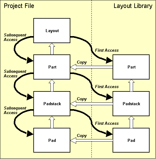
Figure 4-3: Layout Library Access
Changing the library path setting is meaningful only if a series of different part symbols are to be loaded from a library file which is not accessible through the predefined library path. Use the following commands to set the library path to the
demolib.ddb DDB file of the current directory:
| Settings | |
| Select Library | |
| Library Name ('c:/baelib/stdsym.ddb') ? | demolib |
With the commands above, the library path is set to the
demolib.ddb DDB file of the working directory, i.e., requested part symbols on subsequent load operations will be copied from
demolib.ddb.
Placing Parts
The
,
and
functions from the
menu are used for placing parts. These functions work on the selected part set. Initially after loading a layout, all parts are selected, i.e., the system behaves as usual. The functions from the
submenu can be used to restrict and/or redefine the set of parts selected for placement. The
function issues a
All parts have been placed already! message if all parts are already placed or a
All selected parts have been placed! message if all selected parts are already placed, but there are still unselected parts which have not yet been placed. The part set selection popup window displays placed selected parts as
[ name ], placed unselected parts as
( name ), unplaced selected parts as
: name and unplaced unselected parts as
< name >. See
chapter 4.4.1 for more information on part set definitions.
The
function is used to load and place parts on the current layout. On layout hierarchy level, the
function activates a net list part name popup menu with the part name prompt. This popup menu displays placed net list parts in brackets
([,
]). Unplaced net list parts are preceded by a colon
(:). When selecting or specifying an unplaced net list part name, this part is loaded for placement. Selecting an already placed net list part prompts for confirmation to replace the placed part. Entering an empty string to the part name prompt or selecting the
button loads the next unplaced net list part. This feature is also provided with the
function and works until all net list parts (from the part set) are placed. The system prompts for the library element name when specifying a part name which is not defined in the net list (e.g., when placing a constructive part). Popup menus are provided with the library element name query for selecting the library file and the library element name. The library file name list is derived from the layout library path defined with the BAE setup, i.e., all DDB files available in the directory of the layout library path are listed. The
button or
> input to the library file name prompt selects the standard layout library defined through the
function from the
menu. The
button in the library file name popup selects the current project file. A library element name query is activated after selecting the library file. Library elements can optionally be selected by typing both the library file name (i.e., one of the names displayed with the library file name popup), a slash
(/), and the library element name to the library element name prompt (typing
? for the element name activates a popup menu providing the list of library elements from the specified library file). An empty string input to the library element name query causes the system to use the library element previously selected with the
function (if there was already one specified).
The net list part name selection popups are also provided with the
and
functions from the
menu. The library element name selection of the
function is also implemented for placing pins (i.e., selecting padstacks) on layout part symbol level and for loading pads onto layout padstack level.
Use the following commands to load the part named
IC10 and place it at coordinate [1.2",1.8"]:
| Parts | |
| Add Part | |
| Part Name ? | ic10 |
| Move to [1.2",1.8"] | |
The
function checks whether a part with the specified name exists in the net list. If the part is defined in the net list, then the system knows the package to be used for this part and automatically loads the corresponding part symbol (i.e.,
dil14 in the example above). The system issues an error message such as
Element not found!
if the requested part symbol is not available in the current job file or in the selected library. In this case you should use the
function from the
menu in to check whether the correct library is accessed.
Use the following commands to load and place two parts named
hole1 and
hole2 using the
hole3mm package type which was created in
chapter 4.2.3 in DDB file
demo.ddb:
| Parts | |
| Add Part | |
| Part Name ? | hole1 |
| Library Element Name ? | hole3mm |
| Move to [0.4",0.3"] | |
| Add Part | |
| Part Name ? | hole2 |
| Library Element Name ? | |
| Move to [0.4",2.5"] | |
The (constructive) parts
hole1 and
hole2 are not defined in the net list, i.e., the system does not know the corresponding package types. The
function activates a library element name query with a popup menu providing access to all library files available through the predefined default library path. The
button of this menu can be used for accessing the job-specific library of the currently processed DDB file. After selecting the library file, another popup menu with a list of all symbols available in the selected library file is activated. An empty string input (i.e., just pressing the return key
) to the library element name query causes the system to use the part symbol loaded with the preceding
call.
Use the following commands to load and place the plug named
x1000:
| Parts | |
| Add Part | |
| Part Name ? | x1000 |
| Rotate Left | |
| Move to [2.4",1.0"] | |
Pressing the right mouse button during part placement activates a submenu which provides functions for specifying absolute placement coordinates, part rotation (even at arbitrary rotation angles) and part mirroring (for placing SMDs on solder side).
Use the following commands to place the next part:
| Parts | |
| Add Part | |
| Part Name ? | |
| Mirror On | |
| Move to [1.8",1.4"] | |
An empty string input (i.e., just pressing the return key
) to the part name query causes the
function to load the next unplaced net list part. In the example above, the system automatically loads the SMD capacitor named
c100, which then is placed on solder side.
The facility for loading the next net list part (without knowing the corresponding part name) can also be activated with the
function. Use this command to place the part named
c101 as in
| Parts | |
| Place Next Part | |
| Mirror On | |
| Move to [1.4",1.4"] | |
Use the following commands to place the relay part named
k1, the resistor parts named
r100,
r101,
r102,
r103,
r104,
r105 and the switch named
s1000:
| Parts | |
| Place Next Part | |
| Move to [0.8",0.8"] | |
| Place Next Part | |
| Move to [1.0",2.4"] | |
| Place Next Part | |
| Move to [1.6",2.4"] | |
| Place Next Part | |
| Rotate Left | |
| Move to [1.6",1.2"] | |
| Place Next Part | |
| Rotate Left | |
| Move to [1.4",1.2"] | |
| Place Next Part | |
| Move to [2.1",2.1"] | |
| Place Next Part | |
| Move to [2.1",1.8"] | |
| Place Next Part | |
| Rotate Right | |
| Move to [0.2",2.3"] | |
The
function can be utilized for subsequently placing a series of parts at certain rotation angles and/or mirror modes (e.g., SMD parts). Use the following commands to set the standard placement rotation angle to 270 degrees and place the switches named
s1001 through
s1009:
| Parts | |
| Set Default Angle | |
| 270 Degrees Left | |
| Place Next Part | |
| Move to [0.2",2.1"] | |
| Place Next Part | |
| Move to [0.2",1.9"] | |
| Place Next Part | |
| Move to [0.2",1.7"] | |
| Place Next Part | |
| Move to [0.2",1.5"] | |
| Place Next Part | |
| Move to [0.2",1.3"] | |
| Place Next Part | |
| Move to [0.2",1.1"] | |
| Place Next Part | |
| Move to [0.2",0.9"] | |
| Place Next Part | |
| Move to [0.2",0.7"] | |
| Place Next Part | |
| Move to [0.2",0.5"] | |
Use the following commands to complete the placement, i.e., place part
v1 (with absolute placement coordinates and 45 degree rotation angle) and part
v1000:
| Parts | |
| Place Next Part | |
| Set Angle | |
| Angle (Deg./(R)ad) ? | -45 |
| Jump Absolute | |
| Absolute X Coordinate (mm/") ? | 0.825" |
| Absolute Y Coordinate (mm/") ? | 1.225" |
| Place Next Part | |
| Move to [1.2",1.6"] | |
| Place Next Part | |
The
function issues the
All parts have been placed already!
message once all net list parts are placed. I.e., the
function can also be used to check on placement completion.
After correctly executing all work steps of this chapter, the PCB layout example should look like the one shown in
figure 4-4.
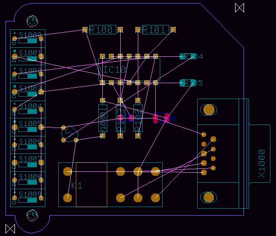
Figure 4-4: Layout with Part Placement
Moving and Deleting Parts
The
function is used to move parts which are already placed on the layout. Pressing the right mouse button during part movement activates a submenu with special options for rotating and mirroring, absolute or relative placement coordinates input, etc. The
function is used to delete placed parts from the layout. You should test these functions on the currently loaded layout and use the
and
functions for estimating design modifications and returning to the original design stage as shown in
figure 4-4.
Alternate Part Package Type Assignment
The
option is provided with the
Layout Editor submenus which can be called by pressing the right mouse button during interactive part placement. This option can be used to change the part package type of the currently placed part. The alternate package type can be selected from a list of layout part macros. The alternate part list is
either pre-defined in the logical library using the
loglib utility program (see
chapter 7.11)
or can be defined through an SCM symbol
$plname attribute value assignment such as
[package1,package2,...]. An error message such as
No alternate part macros defined! is issued if no alternate package types are defined for the currently processed part. An error message such as
Connected pins missing! is issued if the pin definitions on the selected alternate package type do not match the net list, i.e., if net list pins are missing on the selected macro. Alternate part package type assignments create a backannotation request which triggers automatic
when loading SCM plans to the
Schematic Editor (see
chapter 2.7).
requests also prevent the
Packager from forward annotation without confirmation (see
chapter 3.2.3).
Mincon Function, Airlines Display
Unrouted net list connections are displayed as airlines. During part placement, the
function performs dynamic (real-time) recalculation of these airlines to display minimum length airline sets. I.e., the
function is a most useful utility for achieving an optimum manual placement. Use the following commands to test different airline calculation methods supported through the
function and note how the
function type affects the way airlines are displayed:
| Settings | |
| Mincon Function | |
| Corners Horizontal | |
| Mincon Function | |
| Pins Vertical | |
| Mincon Function | |
| Mincon Off | |
| Mincon Function | |
| Corners H+V Sum | |
The
function from the
menu is used to set the airline display mode to be applied during part movement.
switches off the airlines display during part movement.
does not recalculate the nearest connection points during part movement.
dynamically recalculates the closest connection points (note how the airlines jump to the nearest pins or copper corners during part movement).
is the default
option.
The
and
options allow for a net-specific airline display, i.e., it is possible to fade-out
() and/or fade-in
() net-specific airlines by selecting the desired net(s) from a net name popup menu which optionally allows for multiple net selections through net name pattern specifications.
The
option forces the graphical display of all airlines, whilst
fades out all airlines.
The context menu which is available through the right mouse button during part placement provides the
and
options for selecting either part-specific or global airline display.
4.3.3 Text and Graphic
On layout hierarchy level, text (on documentary layers or on signal layers) and graphic (i.e., polygons such as documentary lines, documentary areas, passive copper areas, active copper areas, keepout areas, copper fill workareas) can be defined. For the following operations it is recommended to set the input grid to 1/20 inch (use the
and
functions from the
menu) and to set the coordinate display mode to inch (use function
from the
menu).
Placing Text
Use the following commands to place the
DEMO text string adjacent to the right top of the board outline with a text size of 4mm on the
() documentary layer:
| Text, Drill | |
| Add Text | |
| Document Layer | |
| Insertion Plan | |
| Text ? | DEMO |
| Set Angle | |
| Angle (Deg./(R)ad.) ? | -45 |
| Text Size | |
| Text Size ( 2.54mm) ? | 4 |
| Move to [2.4",2.6"] | |
Use the following commands to place the
Component Side text string with text size 2.54mm on the PCB component side signal layer (Top Layer, Layer n (Parts.)):
| Text, Drill | |
| Add Text | |
| Layer n (Parts.) | |
| Text ? | Component Side |
| Text Size | |
| Text Size ( 4.00mm) ? | 2.54 |
| Move to [1.00",2.55"] | |
The
function which can be activated whilst placing texts sets the default text size for subsequent calls to the
function. Use the following commands to place a rotated and mirrored text with string
Solder Side on the PCB solder side (signal layer 1):
| Text, Drill | |
| Add Text | |
| Layer 1 | |
| Text ? | Solder Side |
| Set Angle | |
| Angle (Deg./(R)ad.) ? | 180 |
| Mirror On | |
| Move to [1.80",2.55"] | |
Texts placed on signal layers are subject to the design rule check. I.e., the DRC will issue distance errors for intersections between signal layer texts and other objects (pads, traces, copper areas, texts, etc.) placed on the same signal layer.
Moving Part Names and Part Attribute Texts
The
function from the
and/or
menu is used to move part names. Use the following commands to move the names of the SMD resistors named
r104 and
r105 on top of the parts:
| Text, Drill | |
| Move Name | |
| Move to "r104",[2.1",2.1"] | |
| Move to [2.1",2.15"] | |
| Move Name | |
| Move to "r105",[2.1",1.8"] | |
| Move to [2.1",1.85"] | |
The
function from the
and/or
menu can be used for moving and/or placing selectable part attributes. Attribute text offsets defined through
override the global text offset set with
. The attribute to be moved is selected through a mouse-click on the attribute text. Since part names are internally stored as
$ attributes, the
function can also be used to move part names without changing the placement of other part attributes.
Part names and part attribute texts of group-selected parts can be reset to their library-defined default positions using the
function implemented with the
gedgroup User Language program.
Measuring
The
Layout Editor automatically activates a measuring function when placing new text with string
#. This function determines the distance between the two input coordinates subsequently to be specified. The resulting text string emerges from the corresponding distance value; the length units (inch or mm) result from the current coordinate display mode selected with the
menu function. Use the following commands to apply measuring on the bottom right board outline edge and place the resulting distance value (2.2") on the
() documentary layer:
| Text, Drill | |
| Add Text | |
| Document Layer | |
| Insertion Plan | |
| Text ? | # |
| Move to Left Coordinate,[0.6",0.3"] | |
| Move to Right Coordinate,[2.8",0.3"] | |
| Move to [1.50",0.15"] | |
Documentary Lines, Documentary Areas
Use the following commands to create a documentary line and two arrow-shaped documentary areas on the
() documentary layer to indicate the previously defined measuring:
| Areas | |
| Add Document Line | |
| Insertion Plan | |
| Move to [0.6",0.15"] | |
| Move to [0.8",0.15"] | |
| Done | |
| Add Document Area | |
| Insertion Plan | |
| Move to [0.6",0.15"] | |
| Move to [0.65",0.2"] | |
| Move to [0.65",0.1"] | |
| Done | |
| Add Document Area | |
| Insertion Plan | |
| Move to [2.8",0.15"] | |
| Move to [2.75",0.2"] | |
| Move to [2.75",0.1"] | |
| Done | |
Passive Copper Areas
Use the following commands to create a circle-shaped passive copper area on signal layer 2:
| Areas | |
| Add Passive Copper | |
| Layer 2 | |
| Move to [0.95",1.6"] | |
| Arc Left | |
| Move to [0.8",1.6"] | |
| Done | |
Active Copper Areas
Use the following commands to create an active copper area on signal layer 1 and assign this copper area to net
Vdd:
| Areas | |
| Add Active Copper | |
| Net Name ? | vdd |
| Layer 1 | |
| Move to [2.4",1.7"] | |
| Move to [2.7",1.7"] | |
| Move to [2.7",2.2"] | |
| Move to [2.6",2.3"] | |
| Move to [2.4",2.3"] | |
| Done | |
Keepout Areas
Use the following commands to define a keepout area on signal layer 1 and a keepout area on signal layer
(keepout areas define layer-specific regions on the PCB where no traces, no copper areas, no texts, etc. are allowed to be placed):
| Areas | |
| Add Keep Out Area | |
| Layer 1 | |
| Move to [1.8",1.2"] | |
| Move to [2.2",1.2"] | |
| Move to [2.2",0.9"] | |
| Move to [1.7",0.9"] | |
| Done | |
| Add Keep Out Area | |
| All Layers | |
| Move to [0.6",2.6"] | |
| Move to [0.6",2.1"] | |
| Move to [0.9",2.1"] | |
| Move to [0.9",2.6"] | |
| Done | |
4.3.4 Traces, Routing
The
menu provides functions for interactive routing on layout and/or part hierarchy level, i.e., for manually creating new traces and for modifying or deleting existing traces and/or trace segments. Arbitrary track widths can be defined for individual trace segments or complete routing paths. Special or critical nets such as the power supply can be pre-routed and then fixed to prevent the
Autorouter from rerouting such nets.
Graphic Control Functions, Input Grid, Display
During manual routing, the system provides a highlight on all objects of the currently routed signal. After completing the routing of a certain connection, the corresponding airline is removed from the display. Short-circuits and distance violations introduced by manual routing are immediately indicated by the Online DRC using highlight and/or distance error boxes.
If you fail to connect certain (off-grid) pins with the current input grid settings, then you should use the
functions for selecting a smaller input grid (or even release the grid lock).
The middle mouse button can be used to activate the
menu at any time during manual routing. I.e., important display options such as zoom scale, grids, colors, etc. can be changed without cancelling the currently active trace edit function.
The
menu also provides the
function for selecting the pick preference layer. The pick preference layer is used to resolve ambiguities at the selection of trace elements placed at the same position but on different layers. The pick preference layer is also the default routing layer when starting to route from a drilled ("All Layer") pad or from a copper-free position. On default, the pick preference layer is set to signal layer 1 (solder side).
The algorithm for picking trace corners and trace segments picks the trace element with minimum distance from the pick point if more than one possible pick element is within snapping distance. This allows for reliable selection of trace elements even when working in (small) zoom overview display modes. The trace pick snapping distance is automatically adjusted to the trace width. I.e., trace elements (of wide traces or in high zoom display modes) can easily be picked without having to hit the trace center line.
Highlight Net
The
function from the
Layout Editor
menu is used to mark all connections of the selected net with a special ("Highlight") color. Any power layer heat-trap circles and isolations of the selected net is included with the highlight display, and isolated pins and active copper areas can also be selected for highlight. Starting a new trace on a passive copper area triggers a highlight for the nets connected to that copper area. The
function works as a toggle. To reset the highlight of a certain net, pin or active copper area, simply re-select that object with the
function. Advanced color support and highlight reset facilities are provided through the
(default mode),
(with highlight color selection) and
(for clearing all nethighlight) options of the
function.
In
BAE HighEnd, the
function causes a highlight and/or de-highlight of the selected nets in all currently loaded plans of the current project file on layout board and schematic sheet level (global net highlight, cross-probing).
Selecting the Via
The
Bartels AutoEngineer layout system utilizes special padstack symbols (vias) for connecting different layers of the PCB. At least one via assignment is required before any routing function (i.e. either a trace function or the
Autorouter) can be activated. Use the following commands to insert the
estk padstack symbol to the currently active via list:
| Parts | |
| Select Via | |
| New/Delete: Via Name ? | estk |
| New/Delete: Via Name ? | |
The
estk padstack symbol is used as pin symbol on the already placed part
v1000 (package type
d04a25). I.e.,
estk is available in the current job file. A series of via padstack definitions are provided with the layout libraries shipped with the BAE software. Usually the padstack symbol named
via can be used as standard via. The via assignments introduced with
are stored with the layout element. The
function issues the following error message if no via is selected:
Default via not defined!
The system is capable of processing several different via definitions at a time in order to support blind and buried vias. The via assignment list can be changed at any time. Previously placed vias will not be affected by via list modifications, i.e., the currently defined via list will apply for the interactive routing of new traces. When changing layers during manual routing the
Layout Editor will automatically place vias with the least possible layer usage (if padstacks are defined and selected to the via list accordingly). The current via assignment list will also be used by the
Autorouter, and, with the use of blind and buried vias, the
Autorouter will minimize layer occupancy as well (this is true for all traces except for fixed traces which will not be processed by the
Autorouter).
Standard Trace Widths
The trace function submenus provide options for toggling between thin and wide default track widths during manual routing (necking). The standard values for these default track widths can be changed with the
function from the
menu, where the options
(default value 0.3mm) and
(default value 1.0mm) are provided. The routing of a new trace always starts with the thin default track width.
Manual Routing
Use the following commands to route from pin
A1 of part
K1 to pin
C1 of the same part (both pins are connected to net
Vdd):
| Traces | |
| Add Trace | |
| Move to "K1.A1",[0.8",0.8"] | |
| Move to Corner Point,[0.8",0.95"] | |
| Move to Corner Point,[1.6",0.95"] | |
| Move to "K1.C1",[1.6",0.8"] | |
| Done | |
Each trace corner point is set by pressing the left mouse button. The routing of a trace path is completed with the
option from the submenu available with the right mouse button. This submenu is also available during trace editing with functions such as
or
where the routing layer or the track width can be changed, arc-shaped trace segments can be created, relative and absolute coordinate input can be specified, etc.
Use the following commands to connect the pins
C2 and
C1 of part
K1 with a trace segment on signal layer 2:
| Traces | |
| Add Trace | |
| Move to "K1.C2",[1.6",0.5"] | |
| Layer 2 | |
| Move to "K1.C1",[1.6",0.8"] | |
| Done | |
Use the following commands to create a trace segment on signal layer 1 starting at pin
9 of the plug named
X1000 and ending with a via to connect to the previously generated trace:
| Traces | |
| Add Trace | |
| Move to "X1000.9",[2.45",0.85"] | |
| Move to Corner Point,[2.45",0.65"] | |
| Move to Vertical Trace Segment,[1.6",0.65"] | |
| Layer 2 | |
| Done | |
Use the following commands to deselect
estk from the via list, select the padstack symbol
via (which has been created in
chapter 4.2.2 in the
demo.ddb DDB file) to the via list, and then route a trace on signal layer 2 starting at pin
K of the diode named
V1000 and ending with a via connecting to the horizontal trace between the pins
A1 and
C1 of part
K1:
| Parts | |
| Select Via | |
| New/Delete: Via Name ? | estk |
| Please confirm (Y/N) ? | y |
| New/Delete: Via Name ? | via |
| New/Delete: Via Name ? | |
| Set Edit Layer | |
| Layer 2 | |
| Traces | |
| Add Trace | |
| Move to "V1000.K",[1.2",1.6"] | |
| Move to Corner Point,[1.1",1.6"] | |
| Move to Horizontal Trace Segment,[1.1",0.95"] | |
| Layer 1 | |
| Done | |
You should now gain more practice by using the trace functions on the currently loaded layout in order to create and/or modify more traces (move, cut and delete trace segments; insert, move and delete trace corner points; change track widths, create arc-shaped traces, etc.). Note the
,
and
options provided with the submenu of the
function. The
default mode just moves the corner points of the processed trace segment, whilst the
mode also rearranges adjacent trace segments in order to keep the angles between the processed trace and the adjacent segments constant.
considers intersection points between new and neighbouring segments and rearranges neighbouring segments accordingly. This feature is especially useful for moving diagonal segments at trace corners. The
option is applied if neighbouring segments cannot be rearranged. Use the
and
functions to estimate design modifications and return to the original design stage.
Fixing Traces
It is recommended to fix pre-routed traces which must not be modified and/or rerouted by the
Autorouter. Use the following commands to fix all prerouted traces of net
Vdd:
| Traces | |
| Fix Trace/Net | |
| Net | |
| Move to Signal/Net "Vdd",e.g.[2.0",0.65"] | |
The
function is used to release fixed traces or nets. During fix and release operations the
Layout Editor provides a specific highlight for indicating currently fixed elements.
The Layout Editor trace functions for interactive routing keeps traces and vias fixed when processing pre-routed fixed traces. I.e., when manipulating pre-routed fixed traces, there is no need of re-fixing such traces to prevent the
Autorouter from re-routing and/or rejecting pre-routed traces.
4.4 Autoplacement
The BAE layout system is equipped with powerful
Autoplacement functions. The part set functions are used for selecting and/or deselecting parts for subsequent placement operations. The matrix placement facilities are used for placing selectable part sets onto definable placement grids. Initial placement functions are provided for performing fully automated part placement. The system also provides placement optimization functions for automatic part and pin/gate swap.
The
Autoplacement functions are available from the
,
and
submenus of the
Layout Editor
menu.
Start the
Layout Editor if it is not yet active and load the layout
board from the
demo.ddb DDB file.
Use the
function from the
menu to delete the resistors named
r100 and
r101, and apply group functions to delete the switches named
s1000 through
s1009:
| Parts | |
| Delete Part | |
| Move to "r100",[1.0",2.4"] | |
| Delete Part | |
| Move to "r101",[1.6",2.4"] | |
| Groups | |
| Group Polygon | |
| Parts | |
| Select | |
| Move to [0.1",0.4"] | |
| Move to [0.6",0.4"] | |
| Move to [0.6",2.4"] | |
| Move to [0.1",2.4"] | |
| Done | |
| Delete Group | |
Autoplacement features and functions are used throughout the following sections to place the deleted parts back onto the layout.
4.4.1 Part Set
The
submenu provides features for selecting the parts to be subsequently placed. Parts can be selected and/or deselected according to set principles either by specifying part names
(c1,
r2,
ic15, etc.) or by specifying package types
(dil14,
so20,
plcc44, etc.), where wildcards are also permitted. The user can also select parts from certain blocks of a hierarchical circuit design. With the Part Set functions the user is able to control the placement process in a way that e.g., first the plug(s) can be placed, then the DIL packages, then the capacitors, etc.
Use the following commands to deselect all unplaced parts:
| Parts | |
| Part Set | |
| All | |
| Deselect | |
| Deselect all parts ? | j |
| Abort | |
Now you might want to use the
command to have a look at the part list:
| Parts | |
| Part Set | |
| List Parts | |
The
function provides verbose output of all net list parts:
File : demo.ddb  Layout : board  Parts : 23


 : c100   chip1210  P  : c101   chip1206  P  : ic10   dil14     P
 : k1     relais    P  : r100   r04a25    U  : r101   r04a25    U
 : r102   r04a25    P  : r103   r04a25    P  : r104   minimelf  P
 : r105   chip1206  P  : s1000  s1dilo    U  : s1001  s1dilo    U
 : s1002  s1dilo    U  : s1003  s1dilo    U  : s1004  s1dilo    U
 : s1005  s1dilo    U  : s1006  s1dilo    U  : s1007  s1dilo    U
 : s1008  s1dilo    U  : s1009  s1dilo    U  : v1     to92      P
 : v1000  d04a25    P  : x1000  xsubd9bl  P  - End -
Each part is listed with part name, library name and placement status, respectively. The placement status is indicated using either of the characters
U,
P or
S.
U indicates that the part is neither placed nor selected for placement.
P indicates that the part is already placed on the layout.
S indicates that the part is not yet placed but selected for subsequent placement operations. Press
X and the return key
to exit from the parts list.
Use the following commands to select all unplaced parts with part names starting with an
r:
| Parts | |
| Part Set | |
| Part(s) | |
| Select | |
| Part Name ? | r* |
| Part Name ? | |
The
and
part set selection options from the
function also provide a popup menu for part selections. With the
option, the popup menu only displays unselected parts, whilst with the
option, only selected parts are displayed. A part name pattern can be entered for part set selections.
The above commands selected the two resistors
r100 and
r101 for subsequent placement operations. You can check this with the
function (see placement status
S for these two parts).
The
function can be used to select all unplaced parts for placement. The
function can be used to select parts with library names (such as
so16 for all unplaced 16 pin small outline package types or
dil* for all unplaced dual-in-line package types). The
option can be used to deselect parts from the set of parts to be subsequently placed.
The
and
functions from the
menu can be used for selecting and/or deselecting parts which are defined in certain blocks of a hierarchical circuit design. I.e., parts are selected or deselected through block names. Part block names are automatically transferred and stored by the
Packager utilizing the internal
$blkname part attribute.
It has already been mentioned that the
and
functions work on the part set (see section Placing Parts in
chapter 4.3.2). Use the following commands to set the coordinate display mode to inch, and place all parts of the currently defined part set (i.e., the two resistors named
r100 and
r101):
| Settings | |
| Coordinate Display | |
| Display Inch | |
| Parts | |
| Place Next Part | |
| Move to [1.0",2.4"] | |
| Part | |
| Place Next Part | |
| Move to [1.6",2.4"] | |
| Parts | |
| Place Next Part | |
The
function issues the
All selected parts have been placed already!
message if no more part is selected for subsequent placement operations anymore (i.e., all parts of the previously defined part set are already placed).
4.4.2 Matrix Placement
Matrix placement is a special initial placement process for automatically placing selected parts on certain matrix-defined insertion positions.
Use the following commands to select all parts with library name
s1dilo (i.e., the switches named
s1000 through
s1009) for subsequent placement operations:
| Parts | |
| Part Set | |
| Select Macro | |
| Select | |
| Library Element Name ? | s1dilo |
| Library Element Name ? | |
Set the default placement rotation angle to 270 degree (without mirroring (the
option is probably located in the
group of the
dialog from the
menu when working with customized BAE user interfaces):
| Parts | |
| Default Angle | |
| 270 Degrees Left | |
Use the following commands to define a placement matrix, place all selected parts onto this matrix and delete the placement matrix definition again:
| Parts | |
| Matrix Placement | |
| Define Matrix | |
| Move to Matrix Origin,[0.2",2.3"] | |
| Move to Matrix Element Size Designation,[0.3",2.1"] | |
| Move to Matrix Size Designation,[0.2",0.5"] | |
| Place Matrix | |
| Delete Matrix | |
The
function automatically places all parts of the currently defined part set onto the placement matrix, also considering the current default placement rotation angle and mirror mode settings.
Now all net list parts are placed. You might want to check this with the
function.
4.4.3 Initial Placement
The
system provides full automatic initial placement algorithms. The initial placement functions automatically place all unplaced net list parts inside the board outline onto the currently selected input (placement) grid, considering pre-placed parts (connectors, LEDs, etc.), keepout areas and net list preferences, and also featuring automatic block capacitor and SMD device recognition. Automatic SMD part mirroring can optionally be enabled to allow SMD placement on the solder side. Either unrestricted or restricted automatic part rotation in 90 degree steps can be applied; restricted part rotation can be used to simplify subsequent insertion processes. A generally applicable part expansion value can optionally be defined to ensure minimum clearance between adjacent parts. The placement algorithms are guarded by adjustable strategy parameters for net list preference control and for the consideration of part segment matching/fitting. Rip-up and retry passes are automatically applied during the placement process to optimize board area yield.
The initial placement routines are integrated to the
submenu which provides the following functions:
| Parts | |
| Auto Placement | |
The
,
and
function can be used to perform automatic part placement.
Only the parts from the current part set (see
chapter 4.4.1) are placed. Placed parts which are not selected to the current part set are treated like fixed parts. This feature allows for automatic placement of selectable part groups.
The first part selected for placement will be positioned at the placement start point. The
function automatically designates the placement start point. The
and
functions prompt the user for the placement start point (prompt
Select placement start point!). The placement of the first part determines the placement of subsequent parts. I.e., the selected placement start point position has crucial meaning for the complete placement process (with regard to 100% completion success and/or the quality of the achieved placement). If the first part cannot be placed at the placement start point, then no subsequent part can be placed either. If the placement start point is selected outside the board outline, then no part can be placed at all. If no board outline is defined then there are no restrictions on selecting the placement start point, however parts could then be placed even outside the boundaries of the currently loaded layout element.
After starting an initial placement function the placement progress is indicated in the status line by a progress message such as
Pass : 1/1 Part : <p>/<n>. The autoplacement process can be stopped by keystroke. Each autoplacement stop request is verified with user confirmation and will be denoted by a message such as
Autoplace aborted!. Note that there might be a short delay on stop requests since any currently active autoplacer rip-up and retry pass must be completed.
A message such as
Operation completed without errors. is issued after completing an initial placement function to indicate that all parts have been successfully placed. If the autoplacer fails to complete 100% part placement using the current parameter settings, then a message such as
<n> parts could not be placed! is issued, denoting the number
<n> of yet unplaced parts. On incomplete initial placement it is recommended to change placement parameters (use smaller placement grid, reduce part expansion, use unrestricted part rotation, allow SMD mirroring; see below on how to set placement parameters) and restart the autoplacer (after
and/or selecting a different placement start point) to achieve 100% part placement.
Full Autoplacer
The
function performs cluster placement (see below) with automatic placement start point selection and subsequently applies multi-pass placement optimization (see
chapter 4.4.4 below) using the currently selected placement optimization parameters (number of passes and the pin/gate swap method). The placement start point results from the board outline gravity point. No part can be placed using the
function, if the board outline gravity point is outside the board outline (e.g., on L-shaped PCBs) then ; in this case either
or
must be used instead of
.
If no board outline is defined, then the placement start point results from the absolute origin of the currently loaded layout element. In this case it is recommended to zoom to overview after completing the placement process since parts can be placed beyond the currently defined and/or visible layout element boundaries.
Cluster Placer
After activating the
function the user is expected to select the placement start point interactively. The first part selected for placement is positioned at the placement start point.
The
function analyzes the net list to classify the nets and parts contained in the net list. Parts are grouped to clusters, and these clusters are subsequently placed on the layout with respect to pre-calculated cluster-dependent placement priorities. Each cluster is grouped by selecting a multi-pin part and a series of connected parts with less than four pins. Parts which are connected to power signals only (such as block capacitors) are postponed during cluster generation and will be assigned to clusters with corresponding power connections afterwards. This method of cluster building automatically involves block capacitor recognition, thus featuring appropriate block capacitor placement nearby corresponding ICs. Parts and/or part clusters are assigned and/or processed due to alphabetical part name order. It is recommended to introduce part type grouping by choosing appropriate type-specific part name patterns, i.e., to insert connectors at the end of the part name list to avoid block capacitor assignment to connectors and/or plugs (e.g., by using name pattern
x??? for connectors and/or plugs,
ic??? for integrated circuits, etc.).
Area Placer
The
function performs area placement with interactively selectable placement start point. Area placement does not consider any net list preferences, i.e., only part dimensions are considered as placement criteria. The
function can be used to estimate part placement area requirements, i.e., to check whether the board area is large enough to place all parts.
Part Pin Factor
The part pin factor is used to control the sequence of parts and/or clusters to be placed. The next part to be placed is selected by applying a combination of two strategies. The first strategy simply selects the part with the maximum number of pins connected to already placed parts. The second strategy selects the part with the maximum ratio of number of part pins connected to already placed parts to total part pin count. The part pin factor value designates which strategy has higher priority. Use the
| Parts | |
| Auto Placement | |
| Settings | |
| Part Pin Factor | |
| Pin Count Weight [0.0,1.0] (0.90) ? |
function to set the desired part pin factor value in the range 0.0 (for considering connection counts only) to 1.0 (for considering connection count to total pin count ratios only). On default the part pin factor value is set to 0.9. A high part pin factor value usually results in a better distribution of nets, but could cause excessive placement area fragmentation on high-density layouts by early placement of small parts, which might prevent from placing larger parts afterwards.
Segment Fit
The segment fit value is used to control on how much part edge length matching should be considered by the placement algorithm, i.e., whether preference should be given on placing parts with equal edge lengths side by side. Use the
| Parts | |
| Auto Placement | |
| Settings | |
| Segment Fit | |
| Segment Fit [0.0,1.0] (0.10) ? |
function to set the weight factor for considering part edge length matching. Valid segment fit values are in the range 0.0 (no segment fit preference) to 1.0 (high segment fit preference). On default the segment fit value is set to 0.1. High segment fit values usually result in better looking layouts, and can increase the routability of layouts with many bus connections. Better routability of high-density layouts with a "random" connection distribution however can be achieved using smaller segment fit values.
Mirroring Mode
The part mirroring mode has effect on the placement of SMD parts only. With the
default option, SMD parts can only be placed on the PCB part side.
is used to allow unrestricted placement of SMD parts on both the part side and the solder side. The
option restricts automatic part mirroring to 2-pin SMDs only, thus allowing for solder side placement of small parts such as block capacitors whilst placement of SMDs with more than 2 pins is forced onto the PCB part side. Use the
| Parts | |
| Auto Placement | |
| Settings | |
| Mirroring Mode | |
function to select the desired SMD mirroring option.
Rotation Mode
The part rotation mode is used to apply either unrestricted or restricted automatic part rotation in 90 degree steps. With the
default option all parts can be placed at arbitrary 90 degree rotation steps. Option
can be used to restrict part rotation, i.e., to allow no rotation or 90 degree left rotation only. Restricted part rotation can be used to simplify subsequent insertion processes which will also result in a reduction of CPU time required by the placement algorithms. Use the
| Parts | |
| Auto Placement | |
| Settings | |
| Rotation Mode | |
function to select the desired part rotation mode.
Part Size, Part Expansion, Block Capacitors, Placement Grid
The parts are placed onto the currently selected input grid (to be set using the
function from the
menu). The placement area required for each part (i.e., the part size) emerges from the element boundaries of the corresponding part macro. This should be taken into consideration at the definition of element boundaries when creating part macro symbols. It is recommended to refrain from defining unnecessarily large part macro element boundaries to avoid redundant placement area occupancy.
A generally applicable part expansion value can optionally be defined in order to ensure minimum clearance between adjacent parts (on low-density layouts). Use the
| Parts | |
| Auto Placement | |
| Settings | |
| Part Expansion | |
| Expansion Value ( 0.00mm) ? |
function to set the desired part expansion value. On default the part expansion value is set to 0.0mm (i.e., no part expansion is applied). Note that the specified part expansion value with no regard to different part macro type dimensions is equally applied on each part macro type except for block capacitors. Block capacitors are automatically recognized and will be placed as close as possible to the ICs to be supplied. The
preferably places block capacitors either on top or on the right-hand side of the integrated circuits, according to the ICs orientation.
The
features a function for automatically reducing part expansion settings by 25 percent steps until either complete placement is achieved or part expansion is reduced to zero.
Rip-up and Retry Passes
The initial placement algorithms are designed to consider only connections to/between already placed parts. Intermediate placement results might show up with alternate positions to be more optimum for a series of previously autoplaced parts. For this reason, rip-up and retry passes are activated for replacing already placed parts in order to find a more optimum placement. Note that preplaced unfixed parts are also processed by the rip-up and retry passes. It is strongly recommended to fix those preplaced parts which must not be replaced. Parts can be fixed using
Layout Editor group functions. Use the
| Parts | |
| Auto Placement | |
| Settings | |
| Number of Retries | |
| Number of Retries [0,9] ( 2) ? |
function to specify the number of retry passes to be applied during the autoplacement process. Two retry passes are used on default; i.e., one rip-up and retry pass is applied after placing half of the unplaced parts and one rip-up and retry pass is applied at the end of the autoplacement process. It is recommended to refrain from specifying too many retry passes since this not only increases CPU time requirements but also can result in a deterioration of intermediate placement results since small parts such as block capacitors might not be correctly replaced with their clusters.
4.4.4 Placement Optimization
The placement optimization features of the
BAE layout system include functions for automatic part and pin/gate swap. The part swap facility mutually exchanges identical components at their insertion position in order to minimize unroutes lengths. The pin/gate swap facility analogously performs an iterative exchange of gates and/or pins and pin groups, where gates or groups can also be swapped between different parts. The admissibility of pin/gate swaps is fairly controlled with appropriate library definitions. Either single pass or multi pass optimization can be applied. Different swap methods can be selected through the
function, with the default
option to perform both component and pin/gate swap,
to switch off pin/gate swap and
to switch off component swap. Applying placement optimization usually causes a significant simplification of the routing problem, thus considerably reducing runtime at the subsequent Autorouting process.
Use the following commands to perform a triple-pass placement optimization with both component and pin/gate swaps:
| Parts | |
| Auto Placement | |
| Settings | |
| Number of Passes | |
| Number of Passes : 2 (1..99) ? | 3 |
| Multi Pass Optimizer | |
During optimization a status line message instantly reports the number of parts processed by the current optimizer pass. Placement optimization can be interrupted at any time by pressing an arbitrary key on the keyboard.
Wait until all optimizer passes are completed and use the
function to estimate how placement optimization did change the complexity of the "ratsnest" (unroutes).
Fixed parts are excluded from placement optimization. It is strongly recommended to fix critical parts before running the placement optimization. Critical parts are those which must not be replaced (e.g., plugs, switches, LEDs, etc.) or where pin/gate swaps are not allowed (e.g., relays, multi-opamps, etc.). Parts can be fixed using
Layout Editor group functions. Please note that automatic pin/gate swap should only be performed if all of the swap definitions stored with the logical library are permitted. Select the
option from the
function to switch off automatic pin/gate swap if you are in doubt about the correctness of swap definitions. Consider please that usually no pin/gate swap is allowed for plugs. Swaps for parts with special attribute values (e.g., resistor networks with attribute
$val must be defined internal to prevent the system from swapping gates between parts with different values. See
chapter 7.11 of this manual for a description of the
loglib utility program and how to introduce pin/gate swap definitions to the logical library.
4.5 Autorouter
With real jobs you should make sure that all of the required power layers are defined (use the
function from the
Layout Editor
menu), the top signal layer setting is correct (use the
function from the
Layout Editor
menu) and pre-routed critical traces such as power supply are fixed, before starting the autorouting process. After finishing the autorouting, you should always run a
from the
Layout Editor before generating manufacturing data with the
CAM Processor.
The user interface of the
Bartels Autorouter is similar to the one of the
Layout Editor. The
Bartels Autorouter provides standard autorouting functions (full and initial routing, rip-up and retry routing, optimizer) and a series of enhanced placement and routing features such as automatic pre-placement with placement optimization, single net routing, net-group routing, component routing, area and/or block routing, mixed-grid routing, selective component and pin/gate swap during rip-up routing, etc. The
Autorouter version provided with the
BAE HighEnd system provides powerful autorouting technologies based on patented neural network technology. The
BAE HighEnd Autorouter supports skilled analogue signal routing, automatic microwave structure generation, grid-less object-orientated routing with automatic placement optimization, etc. The
BAE HighEnd Autorouter also provides features for routing problem recognition and/or classification and for learning and automatically applying problem-adapted routing strategies and/or rules.
4.5.1 Starting the Autorouter
The
function from the
Layout Editor
menu is used to start the
Autorouter. After activating this function, the system automatically saves the currently loaded layout and the
Autorouter program module starts. The
Autorouter automatically re-loads any previously loaded layout.
The layout requires a board outline definition (to be defined with the
function from the
Layout Editor
menu) and a valid via assignment list (use function
from the
Layout Editor
menu). Before starting any autorouter procedure, all net list parts must be placed with correct package types inside the board outline (no part or pin neither any pre-routed trace or via can be placed outside the board outline).
The following error messages might be issued when activating an
Autorouter procedure:
| Board outline not defined! |
|---|
| Cause: | PCB board outline definition is missing |
| Fix: | Layout Editor - - - ... |
| Default via not defined! |
|---|
| Cause: | no via assignment |
| Fix: | Layout Editor - - - ... |
| Parts not found or of different type! |
|---|
| Cause: | not all net list parts are placed on the layout or there are net list parts placed with wrong package types |
| Fix: | use Layout Editor - - to remove net list parts with wrong package types; then use manual or interactive placement functions to complete the part placement |
| Pin out of border (<partname>) ! |
|---|
| Cause: | net list part(s) and/or net list part pin(s) placed outside board outline |
| Fix: | correct part placement |
| Via out of border! |
|---|
| Cause: | pre-placed, fixed via(s) placed outside board outline |
| Fix: | unfix and/or delete via(s) outside board outline |
| Trace out of border! |
|---|
| Cause: | pre-routed, fixed trace(s) placed outside board outline |
| Fix: | unfix and/or delete trace(s) outside board outline |
| Invalid via padstack (cannot use it)! |
|---|
| Cause: | via list contains invalid via definition(s) |
| Fix: | correct via definition(s); there must be at least one via for connecting all signal layers, and each via must contain a drill hole and pads for at least two adjacent signal layers |
| Double defined padstack! |
|---|
| Cause: | layout contains ambiguous library part definition(s) such as part(s) with more than one padstack placed at the same pin position |
| Fix: | correct library part definition(s) |
| Double defined pad! |
|---|
| Cause: | layout contains ambiguous library pad and/or padstack definition(s) such as pad(s) with more than one copper/connection area or padstack(s) with more than one pad placed on same layer |
| Fix: | correct library pad and/or padstack definition(s) |
Other error messages might be issued if the layout contains short circuits caused by pre-routed fixed traces.
4.5.2 Autorouter Main Menu
The
Autorouter standard/sidmenu user interface provides a menu area on the right side, consisting of the main menu on top and the currently active menu below that main menu. After entering the
Autorouter the menu cursor points to the
function.
The Windows and Motif versions of the
Autorouter can optionally be operated with a pull-down menu user interface providing a horizontally arranged main menu bar on top. The
WINMENUMODE command of the
bsetup utility program is used to switch between
SIDEMENU and
PULLDOWN Windows/Motif menu configurations (see
chapter 7.2 for more details).
The following main menu is always available whilst processing layouts with the
Autorouter:
The functions provided with the
menu allow to use the
Autorouter without fear of causing damage. Up to twenty commands can be reversed or undone using
and then reprocessed with
. This is true even for complex processing such as complete autorouting passes or
User Language program execution.
ensures data security and provides a powerful feature for estimating design alternatives.
The
or
menu can either be activated by selecting the corresponding main menu item or by pressing the middle mouse button. Activation through the middle mouse button is even possible whilst performing a graphical manipulation such as selecting a net or component for routing. The
or
menu provides useful functions for changing display options such as zoom window, zoom scale, input and/or display grids, grid and/or angle lock, color settings, etc.
The
menu of the
Autorouter is equal to the
menu of the
Layout Editor (see
chapters 4.4.3 and
4.4.4). The
Autorouter provides the same initial placement and placement optimization functions as already known from the
Layout Editor, allowing for initial placement and placement optimization to be applied in the
Autorouter without having to go back to the
Layout Editor.
The
menu provides the functions for activating autorouting procedures such as
,
,
,
and
. The
function is used to run a series of router passes previously defined with the
function.
The
menu provides the functions for activating special routing operations such as single net routing, net group routing, component routing, area/block routing, etc.
The
menu is used to set fundamental
Autorouter options for subsequent router passes. These parameters define the design rules and technology requirements to be considered by the
Autorouter (signal layer count, layer assignment, routing grid with half-grid routing option, standard trace width, standard minimum distance, maximum via count, via grid, on-grid or off-grid trace bending, pin contact mode). The parameters defined from the
menu are stored with the layout. Changes to basic routing option parameters (signal layer count, routing grid, toggle half-grid option, standard trace width, standard minimum distance, pin contact mode) cause an automatic router restart (with discard of current routing results) when re-entering some standard autorouting process such as
, initial routing, SMD fan out routing, rip-up routing, optimizing and
.
The
menu provides basic functions for controlling the routing process such as setting the optimizer passes count, activate/deactivate multi-net pattern recognition during rip-up and/or optimization, set the persistence of the rip-up router, activate automatic SMD fan out routing and turn on or turn off automatic security copy.
The
menu provides functions for setting the strategy parameters and heuristic cost factors to be used by subsequent router and optimizer passes (optimizer routing direction, via costs, pin channel costs, counter direction costs, direction change costs, packing costs, dynamic density cost factor, bus bending costs, rip-up distance costs, trace crossing costs, diagonal routing costs, off-grid routing costs).
The
menu provides functions for selecting the layout library, setting the coordinate display mode, selecting the
function for the airline display and activating the automatic design data backup feature.
The
menu provides functions for exiting BAE, returning to the BAE main shell, calling the
Layout Editor and starting
User Language programs. This menu also provides important file management functions such as load and save layout elements or list DDB file contents.
4.5.3 Customized Autorouter User Interface
The BAE software comes with
User Language programs for activating a modified
Autorouter user interface with many additional functions (startups, toolbars, menu assignments, key bindings, etc.). The
bae_st User Language program is automatically started when entering the
Autorouter
bae_st calls the
uifsetup User Language program which activates predefined
Autorouter menu assignments and key bindings. Menu assignments and key bindings can be changed by modifying and re-compiling the
uifsetup source code. The
hlpkeys User Language program is used to list the current key bindings. With the predefined menu assignments of
uifsetup activated,
hlpkeys can be called from the
function of the
menu. Menu assignments and key bindings can be listed with the
uifdump User Language program. The
uifreset User Language program can be used to reset all currently defined menu assignments and key bindings.
uifsetup,
uifdump and
uifreset can also be called from the menu of the
keyprog User Language program which provides additional facilities for online key programming and
User Language program help info management.
The Windows and Motif pull down menu user interfaces of the
Autorouter provide facilities for cascading submenu definitions. I.e., submenus can be attached to other menu items. The
uifsetup User Language program configures cascading submenus for the pulldown menu interfaces of the Windows/Motif
Autorouter modules. This allows for easy submenu function location (and activation) without having to activate (and probably cancel) submenus. The function repeat facility provided through the right mouse button supports cascading menus to simplify repeated submenu function calls.
The following Windows/Motif parameter setup dialogs are implemented for the
Autorouter:
- - : General Autorouter Parameters
- - : Display Parameters
- - : Automatic Placement Parameters
- - : Autorouting Options
- - : Autorouting Control Parameters
- - : Autorouting Strategy Parameters
- - : Autorouting Batch Setup
The
uifsetup User Language program replaces the parameter setup functions of the Windows and Motif pulldown menus with the above menu functions for activating the corresponding parameter setup dialogs.
When using pulldown menus under Windows and Motif, the
uifsetup User Language program configures the following modified
Autorouter main menu with a series of additional functions and features:
4.5.4 In-built Autorouter System Features
Automatic Parameter Backup
The
Autorouter provides an in-built feature for automatically saving important design and operational parameters with the currently processed SCM sheet and/or SCM library hierarchy level. The following parameters are stored to the current design file when activating the
function:
- Autosave Time Interval
- Name of the currently loaded Layout Color Table
- Input Grid
- Display Grid
- Grid/Angle Lock
- Coordinate Display Mode
- Wide Line Draw Start Width
- Part Airline Display Mode
- Library File Name
- Mincon Function Type
Parameter sets are stored using the current layout element name. When loading a layout, the corresponding parameter set is automatically loaded and/or activated, thus providing a convenient way of activating a default parameter set suitable for processing the selected design.
Graphical Output and Status Displays
The current routing result is displayed graphically and through statistical readouts whilst routing is in progress. Graphic output and statistical readout during routing can be deactivated by pressing key
d. The
Router working. Press 'd' to activate display... message is displayed whilst router graphic output is deactivated. Pressing the 'd' key again reactivates the graphic output and the statistical readout. The routing process accelerates by up to 10 percent if graphic output is deactivated. A screen redraw is automatically performed after the routing process has finished.
The number of currently routed connections (compared to the total connection count) and the global via count are continuously reported in the status line whilst during Autorouting processes. Additionally, a routing pass info window for displaying internal routing procedure information is provided on the right side of the
Autorouter user interface. This info window contains a status line for identifying the currently active router pass type
(L - Load Layout,
S - SMD Via Preplacement Pass,
I - Initial Routing Pass,
R - Rip-Up Pass,
P - Optimizer Pattern Search Pass,
O - Optimizer Pass) and the number
n of processed elements in relation to the total number
m of elements to be processed by the current router pass (display
n/m). The status line ends with the current pass number
c and the total number
p of passes to be processed (display
c/p). The values displayed with the router pass status line cannot be used for accurate total routing time predictions since the required time for completing the routing of each net and/or connection strongly depends on the current routing complexity.
The
menu is used to set parameters for controlling graphical output. The zoom functions
(,
,
) are used to select the workspace to be displayed. Usually, one would use
to display the complete
Autorouter work area (i.e. the workspace designated by the board outline).
is the default setting after starting the
Autorouter. The functions for changing the zoom factor
( and
) and the
function can only be executed if layout data is already loaded.
The
function is used to change the current color setup. The
function is used to load a predefined color table. On default, the
Autorouter uses the color table named
standard (from the
ged.dat system file of the BAE programs directory). It is recommended to use a color setup which displays all routing layers. When routing with blind and buried vias, it is also a good idea to change the color setup to distinguish different via types.
The
function is used to set the width at which circuit traces are displayed with their true widths. All traces having a screen width greater than the clipping width are displayed with their true widths. All traces having a screen width less than the clipping width are displayed as center lines. The default clipping width value is 1.5mm.
The
function is used to display connections to active copper areas using either cross-shaped markers on connected pins (option
) or airlines connecting pins and copper area gravity points (option
). On default the
option is used.
User Language
The
Bartels User Language Interpreter is integrated to the
Autorouter, i.e.,
User Language programs can be called from the
Autorouter, and it is possible to implement any user-specific
Autorouter function required such as status display, parameter setup, reports and test functions, CAD/CAM input/output functions, automatic or semi-automatic placement and/or routing functions, customer-specific batch procedures, etc.
The
Autorouter provides both explicit and implicit
User Language program call facilities.
User Language programs can be started with explicit program name specification using the
function from the
menu (empty string or question-mark
(?) input to the program name query activates a
User Language program selection menu).
User Language programs can also be called by simply pressing special keys of the keyboard. This method of implicit
User Language program call is supported at any time unless another interactive keyboard input request is currently pending. The name of the
User Language program to be called is automatically derived from the pressed key, i.e. pressing a standard and/or function key triggers the activation of a
User Language program with a corresponding name such as
ar_1 for digit key
1,
ar_r for standard key
r,
ar_# for standard key
#,
ar_f1 for function key
F1,
ar_f2 for function key
F2, etc.
The
Autorouter environment also features event-driven
User Language program calls, where
User Language programs with predefined names are automatically started at certain events and/or operations such as
ar_st at
Autorouter module startup,
ar_load after loading a design element,
ar_save before saving a design element,
ar_tool when selecting a toolbar item and
ar_zoom when changing the zoom factor. The module startup
User Language program call method is most useful for automatic system parameter setup as well as for key programming and menu assignments. The element save and load program call methods can be used to save and restore element-specific parameters such as the zoom area, color setup, etc. The toolbar selection event must be used to start
User Language programs which are linked to toolbar elements. The zoom event can be used to apply an update request to a design view management feature.
Bartels User Language also provides system functions for performing key programming, changing menu assignments and defining toolbars. These powerful features can be applied for user interface modifications. Please note that a large number of additional functions included with the
Autorouter menu are implemented through the
User Language programs delivered with the BAE software.
See the
Bartels User Language Programmer's Guide for a detailed description of the
Bartels User Language (chapter 4.2 lists all
User Language programs provided with the BAE software).
Neural Rule System
A series of advanced
Bartels AutoEngineer features affecting
Autorouter behaviour and procedures are implemented through the
Neural Rule System. See
chapter 6.3.2 for the rule system applications provided with the PCB layout system.
4.5.5 Autorouter Options
The
menu is used to define the design rules and technology requirements to be considered by the
Autorouter. Option parameters can only be set before starting the Autorouting process (unless otherwise mentioned). On
Autorouter security copies the current option parameter settings are stored to the currently processed job file. I.e.,
Autorouter options need not be redefined on subsequent
Autorouter calls, unless parameter changes are really required for the layout to be automatically routed.
Routing Grid, Standard Trace Width, Standard Minimum Distance
The
Bartels AutoEngineer works as a grid-based router unless the gridless router of the
Autorouter (see below) is activated. The
function from the
menu is used to define the routing grid before starting the Autorouting process.
Table 4-1 lists the selectable standard routing grids.
Table 4-1: Autorouter Grids
| Routing Grid | Via Offset | Standard Trace Width | Standard Minimum Distance |
|---|
| [mm] | [mil] | [mm] | [mil] |
|---|
| 1/20 Inch std. | - | 0.37 | 14.6 | 0.29 | 11.4 |
| 1/40 Inch std. | x | 0.32 | 12.6 | 0.29 | 11.4 |
| 1/50 Inch std. | - | 0.25 | 9.9 | 0.23 | 9.1 |
| 1/60 Inch std. | x | 0.21 | 8.3 | 0.19 | 7.5 |
| 1/80 Inch std. | x | 0.16 | 6.3 | 0.13 | 5.1 |
| 1/100 Inch std. | - | 0.13 | 5.1 | 0.10 | 3.9 |
| 1/40 Inch no ofs. | - | 0.32 | 2.6 | 0.29 | 1.4 |
| 1/60 Inch no ofs. | - | 0.21 | 8.3 | 0.19 | 7.5 |
| 1/80 Inch no ofs. | - | 0.16 | 6.3 | 0.13 | 5.1 |
| 1/100 Inch w. ofs. | x | 0.13 | 5.1 | 0.10 | 3.9 |
The default routing grid setting at the first
Autorouter call for a particular layout is
. Each routing grid change is stored with the layout and also sets the standard trace width and minimum clearance distance values to the default settings for that grid (see
table 4-1 for the grid-specific default values). Both the standard trace width and the standard minimum distance can be changed after specifying a new routing grid (use functions
and
, respectively). Note however that the sum of trace width + minimum distance must not exceed the current routing grid; otherwise the
Autorouter issues an
Incompatible options selected! error message when starting the routing process (note warnings such as
Accepted for smaller default trace width! and/or
Accepted for smaller minimum distance!, and modify trace width and/or minimum distance until either of the messages
Minimum distance value accepted! or
New default trace width accepted! is issued). You should set the trace width and minimum distance values to 0.2mm each if you intend to route an SMD layout with 1/40 inch routing grid, since this allows the
Autorouter to use the pin channels of SO packages.
Note that the 1/60 inch routing grid (i.e., the complete routing matrix) is internally shifted by 1/120 inch, thus enabling the
Autorouter to place two traces between adjacent pins of DIL packages which are placed on 1/10 or 1/20 inch grid.
The
option of the
function can be used to specify arbitrary routing grids such as some metric grid for special pin grids. Arbitrary routing grid settings will set both the standard trace width and the minimum distance to half the value of the routing grid. I.e., a routing grid specification of e.g., 1.1mm will set the trace width and the minimum distance to 0.55mm each.
The built-in off-grid recognition of the
Bartels AutoEngineer allows for off-grid placement of pins and pre-routed traces. I.e., the
Autorouter is able to connect objects which are not placed on the routing grid (e.g., plug pins on metric grid). Note however that on-grid items make the job much easier for the
Autorouter since off-grid routing is quite time-consuming and could even prevent the
Autorouter from connecting certain items in a simple way. It is recommended to use a reasonable grid for part placement to avoid off-grid pin placement and to enable pin channel routing for better routing results.
Please note that smaller routing grids result in quadratic growth of memory requirements for the routing matrix, and that CPU time usage during the Autorouting process rises even more dramatically (due to a non-polynomial growth of the number of possible routing solutions). It is recommended to refrain from selecting unnecessary small routing grids.
Some routing grid options support routing with via offset (see
table 4-1). No via offset means that vias are placed in-line with the traces (i.e., on the routing grid). Routing with via offset means that vias can be shifted by half the routing grid at their placement. The choice to offset or not must be calculated by the user taking into consideration the routing grid, trace width, clearance distance and via size. Routing with via offset may well allow to use channels which would otherwise be occupied by in-line placed vias on adjacent grid channels. This can have a significant negative effect on the routing success (see
figure 4-5 for an illustration). The via offsets are calculated for via diameters smaller than 1mm. It is recommended to refrain from routing with via offset when using larger vias since this could cause poor routing results.
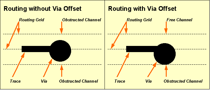
Figure 4-5: Routing with or without Via Offset
The standard trace width is the track width to be used for routing the connections. The standard trace width applies for all nets except for those where certain net attributes are defined. If a
routwidth net attribute value is set for a particular net, then the entire net is routed with that routing width. If a
powwidth value is set for a particular net, then all library-defined power supply pins of that net are connected with that power width. The standard minimum distance sets the default minimum clearance distance to be considered by the
Autorouter when routing the connections. The standard minimum distance applies for all nets, except for those where non-default minimum distance values are assigned with the
mindist net attribute. The
Autorouter automatically performs high priority processing of nets with net attribute values set. The
priority net attribute can be used to specify explicit net-specific routing priorities. See the
loglib utility program description in
chapter 7.11 of this manual for more details on how to use net attributes for controlling the routing process.
Signal Layer Count and Layer Assignment
The
function from the
menu is used to specify the number of signal layers to be simultaneously routed by the
Autorouter. The signal layer count can range from 2 to 12. The default signal layer count for a particular layout corresponds with the top layer setting of that layout.
The
function is used to set the preferred routing direction (horizontal, vertical or all directions) for each routing layer. With the
function it is also possible to define trace keepout layers (i.e., layers where routing is prohibited) or to remove layers from the routing layer list (which will decrement the signal layer count). The default layer assignments are horizontal for layer 1, vertical for layer 2, horizontal for layer 3, vertical for layer 4, etc. Changing the routing layer count with function
resets the layer assignments.
Routing layer numbering starts with signal layer 1 (solder side). The
Autorouter simultaneously routes all routing layers. Single-layer boards can be routed with routing layer count 2 and routing layer 1 defined as prohibited layer.
All objects placed on prohibited layers are considered by the
Autorouter. I.e., via keepout areas on a double-sided layout can be defined by placing keepout areas on signal layer 3 of the layout, setting the routing layer count to 3, and defining routing layer 3 to be prohibited. The
Autorouter would then use signal layers 1 and 2 for routing the traces and refrain from placing vias at positions where via pads would intersect with keepout areas on layer 3.
The layer assignments (except for the signal layer count) can be changed between different router passes, i.e., without the need of restarting the complete routing process. Note however that restrictions introduced with layer assignment changes will never cause a deterioration of the current routing result at subsequent router passes. I.e., the
Autorouter will try to but not necessarily remove all previously routed traces from prohibited layers, if those layers were available for routing before.
Changing layer assignments between different router passes introduces highest flexibility at the routing of complex PCB technologies. Best success at the routing of certain multilayer SMT boards is often achieved when using outside layers (solder and component side) with highest priority for connecting SMD pins to inside signal layers. This can be accomplished with SMD Via Pre-Place passes to be subsequently activated with dynamically adapted layer assignments and increasing routing channel widths (use the
and
functions to apply single router passes). After completing the SMD Via Pre-Placement some Initial passes (with via and/or channel width restrictions) can be applied to route the signal inside layers only (prohibit the outside layers). Finally the outside layers can be released again for subsequent router passes such as Complete Initial pass, Optimizer, rip-up routing, etc.
The
Bartels AutoEngineer is capable of routing up to 12 power layers in addition to the signal layers. I.e., the
Bartels AutoEngineer can rout multilayer designs with a total of up to 24 layers. The power layer routing algorithms are equipped with intelligent power plane detection features for split power plane routing. When routing power layers, the
Autorouter correctly connects SMD pins to power layers and/or active copper areas defined on such power layers.
Maximum Via Count
The
function is used to set the maximum number of vias per circuit trace. The default maximum via count is 20. A maximum via count of 0 forces the
Autorouter to rout the layout without vias. The maximum via count can be changed between different router passes, i.e., without the need of restarting the complete routing process. Note however that restrictions introduced with maximum via count changes will never cause a deterioration of the current routing result at subsequent router passes. I.e., the
Autorouter will try to but not necessarily remove all previously placed vias.
Via Grid
The
function is used to set the grid for placing vias to 1/10 or 1/20 inch. The
option is used on default, thus allowing unrestricted via placement according to the current
setting (see above). The via grid can be changed between different router passes without the need of restarting the complete routing process. Note however that restrictions introduced with the via grid changes will never cause a deterioration of the current routing result at subsequent router passes, i.e., the
Autorouter will try to but not necessarily replace previously placed vias.
Sub-Grid Routing
The
function is used to activate half-grid routing (option
). On default half-grid routing is deactivated (option
). Half-grid routing means that the
Autorouter can alternatively use a routing grid shifted by half of the selected routing grid, e.g., half-grid routing with 1/40 inch routing grid can also utilize the 1/80 inch grid routing grid. The current standard trace width and minimum distance settings are not affected by the sub-grid routing option. Half-grid routing yields better use of regions nearby off-grid placed objects such as pin channels at off-grid placed parts, thus considerably increasing routability of dense layouts.
Gridless Routing Option
A rule-driven gridless router is integrated to the
Autorouter. Gridless routing is deactivated on default (option
of the
function from the
menu). The rule-driven gridless router can be activated through the
option from the
function. The gridless router performs selective gridless routing, i.e., gridless routing is only applied locally where this yields better results in terms of routability and manufacturing optimization. With gridless routing activated, there are much more options for using off-grid pin channels, which might significantly increase the routability of complex layouts. Gridless routing generates straighter connections to off-grid placed pins, thus preventing from blocking adjacent pin channels and also performing more optimization for manufacturing.
The
mode allows for traces to leave the routing grid under virtually any condition and for minimum distance routing between off-grid pins, thus achieving significantly better routing results especially for dense SMT boards.
The
mode straightens connections to gridless placed pins and vias only locally and resumes and/or applies gridbased routing for normal traces. This mode is not capable of routing between offgrid placed pins where this otherwise would be possible in
mode.
Warning
Note that gridless routing requires more main memory and computing power due to additional data structures (gridless priority tree) to be maintained during the routing process.
Traces On-Grid/Off-Grid
The
function is used to set the trace corner cutting mode. On default trace corner cutting falls on half grid points (option
). The
option forces trace corner angles onto the routing grid only, thus ensuring correct spacing between diagonal trace segments and pad corners.
Figure 4-6 illustrates the effects of off-grid and on-grid trace corner cutting.
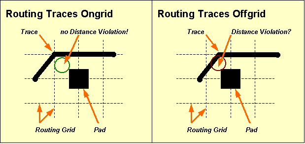
Figure 4-6: Routing Traces Ongrid/Offgrid
Pin Contact Mode
The
function is used to allow (option
, default) or avoid (option
) pin corner routing. This feature works on approximately rectangle-shaped pads and controls whether traces can exit such pads at 45 degree angles or not. Routing with pin corner obstruction can produce better looking layouts, but could also impede 100% routing. Note that connecting pins with a size approximately equal to or smaller than the trace width could fail. The
option should not be used with designs that include thick traces. Note also that bus routing can produce unpredictable results when switched to pin corner obstruction.
4.5.6 Autorouter Control
The
menu provides a series of functions for controlling the routing process.
Optimizer Passes
The
function is used to set the number of Optimizer routing passes to be automatically activated by the
function after obtaining a 100% routing. The Optimizer passes count can range from 0 to 99; 2 Optimizer passes are activated on default.
Router Cleanup, Optimizer Cleanup
The
function is used to activate (default option
) or deactivate (option
) cleanup passes during rip-up routing. The
function is used to activate (default option
) or deactivate (option
) cleanup passes during optimization. When running cleanup passes (note message
Pattern Search issued by the routing progress report), the
Autorouter makes use of a unique pattern search recognition algorithm for identifying disturbing traces during rip-up and cross-net optimization. The
Autorouter is able to select and remove disturbing traces during rip-up and perform cross-net changes during optimization. Cleanup during cross-net optimization requires more computing time, but dramatically reduces via counts and thus is also called if the rip-up router (temporarily) fails to find an acceptable solution. It is recommended to refrain from turning off cleanup when running rip-up on complex designs or optimizing dense boards. Turning cleanup off results in sequential processing of the connections and can produce contenting results when running final Optimizer passes on certain layouts (however, more passes are then required for pushing and/or straightening trace bunches).
Rip-Up Trees, Rip-Up Depth, Rip-Up Retries
The
function sets the maximum number of traces allowed to be simultaneously ripped up per rip-up cycle. The rip-up trees number is set to 2 on default, and can range from 1 to 9. The
function is used to control the persistence of the rip-up process. A high value will result in higher persistence. The rip-up depth value can range from 1 to 999, and is set to 50 on default. The
function sets the maximum number of rip-up retries for routing a particular trace, thus defining the local rip-up router intensity. The rip-up retries number is set to 2 on default, and can range from 0 to 99. Higher rip-up control parameters increase the persistence and intensity of the rip-up routing process, and thus can be used for special problems such as completing 100% routing without intermediate optimizer passes or for routability check.
Once 99.5% routing completion is achieved, the Rip-Up parameters are automatically increased to Rip-Up Trees 6, Rip-Up Level 200 and Rip-Up Retries 10, unless higher values are already set. This helps to avoid the time-consuming Optimizer cleanup passes between Rip-Up passes if only a few open connections are left.
SMD Via Pre-Place
The
function is used to activate (option
) or deactivate (default option
) the initial routing algorithm for connecting SMD pins to signal inside layers. With SMD via pre-placement activated the
function will start with the SMD via pre-place initial routing pass. The SMD via pre-placer will - as far as possible and/or meaningful - generate short trace connections to vias for those SMD pins to be wired. At SMD fanout routing, routing directions result from the shapes and positions of the corresponding SMD pads; i.e., the SMD fanout routing algorithm ignores layer-specific routing direction preferences to refrain from blocking PLCC/SMD pin channels and or PLCC/SMD pins. The SMD via pre-routing pass is intended for preventing the
Autorouter from extensively using the SMD outside layers at an early stage of the routing process, thus involving earlier 100% routing success in a wide range of SMT designs. The SMD via router does not (re-)rout SMD pins which are already connected to fixed traces, and redundant SMD via connections are later eliminated by the Optimizer.
Placement Optimization during Rip-Up Routing
A feature for performing placement optimizations is integrated to the rip-up router of the
Autorouter. The
menu function can be used to activate (option
) or deactivate (option
) placement optimization during rip-up routing. With
, the rip-up router performs pin/gate/groups swaps to increase routability. This can significantly reduce the time required for achieving a 100% autorouting completion. Placement optimization is selective, i.e., swaps with a high potential to simplify the routing problem are carried with higher priority. Swap operations which cause a deterioration of the current routing result rejected by the router's backtracking process. Only unfixed parts are subject to swap operations, and the admissibility of any pin/gate swap is controlled through the corresponding logical library part definitions.
Pin/gate swaps create a backannotation request which triggers automatic
when loading SCM plans to the
Schematic Editor (see
chapter 2.7).
requests also prevent the
Packager from forward annotation without confirmation (see
chapter 3.2.3).
Security Copy
The
function is used to activate (default) or deactivate automatic security copy of intermediate routing results.
4.5.7 Autorouter Strategy
The
menu provides functions for setting routing strategies such as via cost, pin channel cost, packing cost, bus bending cost, dynamic density cost, etc. These settings should be used with care. Only change one or two at a time. Poor routing results are often found to be caused by random strategy parameter settings. The default settings will work best in the vast majority of cases. It is strongly recommended to change strategy parameters in special cases only and to refrain from using extreme values.
There are strong mutual dependencies between different
Autorouter strategy parameters. A high via cost value (for eliminating vias) will necessarily result in more ignorance of routing direction preferences, thus compensating the cost factor for keeping preferred routing directions. Note also that strategy parameters only define subordinate options for the Autorouting process, due to the fact that it is much more important to achieve a 100% routing result instead of, e.g., keeping preferred routing directions. I.e., some cost factors may be completely ignored during initial routing and rip-up and will only be considered by the Optimizer.
Tabelle 4-2 provides an overview to all of the routing parameters which can be set from the Strategy menu.
Table 4-2: Autorouter Strategy Parameters
| Strategy Parameter | Value Range | Default Value | Effect on
Router | Effect on
Optimizer |
|---|
| Optimize Direction | Normal
Preferred
Diagonal | Normal | - | x |
| Via Cost | 2..20 | 10 | x | x |
| Pin Channel Cost | 0..10 | 3 | x | - |
| Counter Dir. Cost | 0..5 | 1 | x | x |
| Dir. Change Cost | 0..5 | 2 | - | x |
| Packing Cost | 0..5 | 1 | x | - |
| Dyn. Density Cost | 0..50 | 10 | x | - |
| Bus Bending Cost | 0..5 | 2 | x | - |
| Distance-1 Cost | 0..10 | 5 | x | - |
| Distance-2 Cost | 0..10 | 2 | x | - |
| Trace Cross. Cost | 2..100 | 20 | x | x |
| Diagonal Cost | 0..10 | 5 | - | x |
| Off-Grid Cost | 0..5 | 2 | x | x |
| Prefered Grid | 0..7 | 0 | x | x |
| Anti-Prefered Grid Cost | 0..10 | 1 | x | x |
Outside Net Type Area Cost
(BAE HighEnd) | 0..5 | 1 | x | x |
Optimize Direction
The
function is used to designate the Optimizer strategy. The
default option causes the Optimizer to ignore layer-specific preferred routing directions in order to obtain the greatest reduction of vias. The
option causes the Optimizer to consider layer-specific preferred routing directions, which could increase the number of vias. The
option causes the Optimizer to prefer diagonal (45 degree) routing where appropriate.
Via Cost
The
setting is used by the Router and the Optimizer. A high via cost factor results in fewer vias but more complex circuit traces. A low via cost factor permits more vias within the restraint of the maximum via count (see above). The via cost value can range from 2 to 20; the default value is 10.
Pin Channel Cost
The
setting is used by the Router only. A high pin channel cost factor results in infrequent use of pin channels. A low pin channel cost factor permits the frequent use of pin channels. Pin channels are the regions between adjacent part pins. The pin channel cost value can range from 2 to 20; the default value is 10.
Counter Direction Cost
The
setting is used by the Router and the Optimizer. A high counter direction cost factor results in strict adherence to the layer-specific preferred routing directions. A low cost factor permits frequent variations from the preferred direction. The counter direction cost value can range from 0 to 5; the default value is 1.
Direction Change Cost
The
setting is used by the Optimizer only. A high direction change cost factor results in less circuit corners. A low direction change cost factor permits frequent changes in routing directions. The direction change cost value can range from 0 to 5; the default value is 2.
Packing Cost
The
setting is used by the Router only. A high packing cost factor results in high bundling of circuit traces. A low packing cost factor will result in wider distribution of circuit traces. The packing cost value can range from 0 to 5; the default value is 1.
Dynamic Density Cost
The
setting is used by the Router only. The dynamic density cost factor controls the global distribution of circuit traces over the entire layout. A high dynamic density cost factor results in a more even distribution of the circuit traces. A low cost factor gives more influence to routing costs. The dynamic density cost value can range from 0 to 50; the default value is 10.
Bus Bending Cost
The
setting is used by the Router only. The bus bending cost factor controls the bending of traces after passing a pin channel. A high bus bending cost factor results in high priority of bending. A low bus bending cost factor results in less bending. The bus bending cost value can range from 0 to 5; the default value is 2.
Rip-Up Distance Cost
The
and
settings are used by the Router during rip-up.
The rip-up distance-1 cost factor controls the use of channels left by ripped up traces in the near distance (0 to 1 grid point). A high distance-1 cost factor results in less use of these channels, thus forcing more local changes during rip-up and retry routing. The rip-up distance-1 cost value can range from 0 to 10; the default value is 5.
The rip-up distance-2 cost factor controls the use of channels left by ripped up traces in the far distance (2 grid points). A high distance-2 cost factor results in less use of these channels, thus forcing more global changes during rip-up and retry routing. The rip-up distance-2 cost value can range from 0 to 10; the default value is 2.
Trace Crossing Cost
The
is used to set the trace transition cost factor, which is considered by the Router and the Optimizer to control cleanup pattern recognition during multi-net optimization. A high trace crossing cost factor allows for a more complex routing with more traces crossing each other, thus also producing more vias. A low trace crossing cost factor leads to increased (and more time-consuming) analysis during cross-net optimization, thus eliminating more vias. The trace crossing cost value can range from 2 to 100; the default value is 10.
Diagonal Routing Cost
The Optimizer considers the
setting on routing layers where the
routing option is selected (see
function above). A high diagonal routing cost factor causes the Optimizer to use more diagonal routes. A low diagonal routing cost factor results in less diagonal routing. The diagonal cost value can range from 0 to 10; the default value is 5.
Off-Grid Routing Cost
The
setting is used by the Router and the Optimizer, and is considered when routing with the half-grid option (see above). A high off-grid routing cost factor results in less use of the sub-grid. A low off-grid routing cost factor permits frequent use of the sub-grid. The off-grid routing cost value can range from 0 to 5; the default value is 2.
Prefered Grid, Anti-Prefered Grid Cost
The
parameter is used for setting a prefered routing grid.
values range from 0 to 7; 0 switches the prefered grid of, higher values cause the router to pefer the use of every 2nd, 4th, 8th, 16th, 32nd, 64th or 128th grid point. The
parameter (value range 1 to 10, default value 1) is used to set a cost factor for routing outside the prefered grid. Prefered grid routing spreads the routing density and takes only effect on layouts with (large) unoccupied areas. Prefered grid routing parameters should be set before the first
Autorouter run. Later changes to these parameters require multiple time-consuming optimizer runs. Note also that high cost factors could cause detouring routes.
Outside Net Type Area Cost (BAE HighEnd)
The
strategy parameter is only supported in
BAE HighEnd. A high cost factor prevents nets from being routed outside their net-specific routing areas, a low cost factor allows for nets to be routed outside their routing areas more frequently. The net area cost factor can range from 0 to 5; the default value is 1.
4.5.8 Autorouter Functions
The
Autorouter supports various routing algorithms and autorouter procedures such as
, initial routing, SMD fanout routing, rip-up/retry routing,
, re-entrant routing, etc. These routing procedures can be activated from the
menu (functions
,
,
,
,
), the
menu
( function) and the
menu
(,
). Activating an autorouting procedure after changing basic routing parameters such as signal layer count, routing grid, half-grid option, standard trace width, standard minimum distance, or pin contact mode discards the currently unfixed traces and vias and (re-)routes the layout with changed options.
The autorouting procedures in
BAE HighEnd are some 30 percent faster than in
BAE Professional. This performance boost is mainly achieved by optimized internal data structures (HighSpeed Kernel) in
BAE HighEnd.
The current routing result is displayed graphically and through statistical readouts whilst routing is in progress. The routing process can be stopped at any time by pressing a key, causing the
Autorouter to revert to the (currently best) routing result.
Single-Pass Initial Routing
The single-pass Initial Router performs signal trace routing considering preferred routing directions, a certain channel width and a maximum via count per two-point connection. The channel width is the maximum permitted deviance from preferred directions. The channel width is specified in routing grid steps. A zero channel width removes the restraints on deviating from the preferred direction, i.e., the entire board area is then released for routing. The maximum via count used by the Initial Router will never exceed the value set with the
function from the
menu (see above). The Initial Router places traces close together, thus using minimum space in order to leave more room for subsequent traces (trace hugging). The Initial Router also uses advanced techniques of copper sharing where appropriate. The Initial Router processes power layer connections and attributed nets (with non-default routing widths, minimum distance settings and routing priorities) with highest priority.
Complete Initial Routing
The Complete Initial Router automatically activates four Initial Router passes to rout all open connections which can be routed without rip-up and retry. With each Initial Router pass the channel width and the maximum via count is increased. The first Initial Router pass runs with maximum via count zero. The last Initial Router pass runs with channel width zero and a maximum via count according to the parameter set with the
function from the
menu (see above).
Rip-Up/Retry Router
The Rip-Up/Retry Router attempts to route all open connections until the board is completely routed. Connections which can be routed without rip-up are routed first. Then the Rip-Up/Retry Router selects and eliminates traces (rip-up) and re-routes them to create space for the unroutes. For this purpose, the router gathers information on dense board areas and increases the cost of routing in such areas. The Rip-Up/Retry Router is supported by a sophisticated array of heuristic strategy parameters. The cost factors can be dynamically adapted to the current routing problem, thus controlling the "price" of strategies such as via placement, routing against preferred directions, using pin channels, etc. It is strongly recommended to refrain from modifying these strategies, unless the routing success is not what would be expected. When changing cost factors, slight adjustments to a few can make significant improvements or make things much worse. The Rip-Up/Retry Router is guarded by a unique backtracking algorithm, which not only prevents from a deterioration of the result or a dead-lock during rip-up or optimization but also is able to exploit a new and/or better routing solution. The Rip-Up/Retry Router automatically activates intermediate Optimizer passes if a single rip-up pass fails to achieve 100% routing success.
Optimizer
The
function is used to start a single
pass. The
usually is applied after 100% routing to optimize the layout for manufacturing. The
eliminates redundant vias, smoothes traces and attempts to rout open connections. Channel width zero is used during optimization and the maximum via count is set to the same value as defined with the
function from the
menu (see above).
SMD Via Pre-Placement
is a special initial routing algorithm for connecting SMD pins to signal inside layers. The SMD via pre-placer generates short trace connections to vias for those SMD pins to be wired. With SMD fanout routing passes, a channel width setting is required and routing directions result from the shapes and positions of the corresponding SMD pads. The SMD via pre-routing pass prevents the
Autorouter from extensively using the SMD outside layers at an early stage of the routing process. This strategy achieves earlier 100% routing success in a wide range of SMT designs. Redundant via connections created by
are later eliminated by the
.
Full Autorouter
The
main menu function is used to start a complete Autorouting process including all router passes such as SMD Via Pre-Placement (optionally), complete initial routing, rip-up/retry routing (if necessary) and optimization. This is the standard procedure for performing complete routing of a board. The number of final
passes can be set with the
function from the
menu (see above). The SMD Via Pre-Placer will only be activated if the
option has been selected with the
function from the
menu.
Batch Setup and Batch Start
The
function from the
Standard Autorouter main menu is used to start a routing process with different user-defined router passes. The
function is used to schedule up to ten of the following autorouting procedures to be subsequently processed with the
function:
| Command |
Routing Pass/Procedure |
|---|
L | |
F | |
I | |
C | |
R | |
O | |
S | |
- | none (remove router pass from batch) |
pass requires a routing channel width specification and a maximum via count setting.
requires a routing channel width specification.
requires the number of required
passes (up to 999).
Single Net Routing
The
function from the
Autorouter
menu activates the single net router. The net and/or connection to be autorouted by the single net router can be selected by mouse-clicking some pin or pre-routed trace of the desired net. The single net router is commonly used for pre-routing power supply signals or critical nets with specific preferences for trace widths, clearance, layer assignments, etc.
Component Routing
The
function from the
menu can be used to rout mouse-selectable parts, i.e., to autoroute all nets connected to the selected component.
Fully Automated Placement and Routing
The
function from the
can be used to activate the
and
function sequence. thus allowing for fully automated layout placement and routing.
Net-specific Airline Display and Net Group Routing
The
from the
menu provides options for controlling net-specific airline display. Nets which are faded-out from airline display are excluded from the autorouting process. Net-specific airline display settings can be changed between router passes. This allows for consecutive router passes to route different groups of nets such as busses of a certain circuit block or signals with certain attributes with specific routing options for preferred routing directions, maximum via counts, etc..
Area/Block Routing in BAE HighEnd
The
Autorouter of
BAE HighEnd considers net-specific routing areas to be defined as documentary areas on signal layers with rule assignments containing a
net_type predicate for the net type. See the
nettype.rul file in the
User Language programs directory
(baeulc) for net type rule definitions. Up to eight different routing area net types can be assigned to each layout. Routing areas and rule assignments (with the
gedrule User Language program) must be defined in the
Layout Editor. Within a routing area, the
Autorouter can only route nets with a matching
$nettype attribute. Nets without
$nettype value or with a
$nettype value different to the
net_type assignment of a certain routing area must not be routed in that area unless they connect to pins inside the routing area. Nets of a certain net type are not restricted to net-specific routing areas, however, they are preferably routed in the corresponding routing areas. Routing outside the net-specific routing area can be controlled with the new
option to be set through the
menu.
4.5.9 Using the Autorouter
Starting the Autorouter
You should first start the
Layout Editor and load the layout
board from the
demo.ddb DDB file. The
command from the
Layout Editor
menu is used to call the
Autorouter:
| File | |
| Autorouter | |
Setting Autorouter Options
The following operations will show how to apply certain router passes for routing our example job using three signal layers. Use the following commands to set the signal layer count to 3:
| Options | |
| Signal Layer Count | |
| 3 Signal Layers | |
Use the following commands to select 1/40 inch routing grid without via offset, and set the standard trace width and the minimum distance to 0.3mm each:
| Options | |
| Routing Grid | |
| 1/40 Inch no ofs. | |
| Trace Width | |
| New Default Trace Width ( 0.32mm) ? | 0.3 |
| Minimum Distance | |
| New Minimum Distance ( 0.29mm) ? | 0.3 |
View, Layout Display
Use the following commands to change trace clipping to 0.1mm and activate the
function:
| V|iew | |
| Set Clipping | |
| Display Traces wider than ( 1.50mm) ? | 0.1 |
| Zoom All | |
Router Batch
Use the following commands to define a router batch process consisting of
with channel width 4,
, and a single
pass:
| Autorouter | |
| Batch Setup | |
| 1: --- | |
| New Batch Pass (L/F/I/S/C/R/O/-) ? | s |
| Initial Pass Channel Width ? | 4 |
| 2: --- | |
| New Batch Pass (L/F/I/S/C/R/O/-) ? | c |
| 3: --- | |
| New Batch Pass (L/F/I/S/C/R/O/-) ? | o |
| Optimizer Passes ? | 1 |
| No Change | |
A dash string input ("-") to the
New Batch Pass prompt can be used to remove the selected router pass from the batch. The sequence of router passes to be processed by
corresponds with the sequence of router passes defined with
. Use the
command to run all router passes previously defined with the
function:
| Autorouter | |
| Batch Start | |
Router batches can also be started with the
button from the
dialog without having to leave the
dialog and subsequently calling the
function.
The routing process for our example starts with
. Subsequently, a
pass is performed. The
will end up with 100% routing success. Finally, one
pass is activated. Each routing pass automatically saves its routing result. The following message is displayed in the status line after finishing the last pass:
Max. 53 of 53 Routes (Pins: 76, Vias: 5)
The layout is now completely routed with 5 vias placed by the
Autorouter.
Optimizer
Use the following commands to run an additional
pass (without pattern recognition, but with high priority for considering preferred routing directions):
| Control | |
| Optimizer Cleanup | |
| Optimizer Cleanup Off | |
| Strategy | |
| Optimizer Direction | |
| Preferred | |
| Counter Dir. Cost | |
| Counter Direction Cost Factor : 1 (0..5) ? | 4 |
| Autorouter | |
| Optimizer | |
Note how the
pass routes traces according to preferred routing directions, albeit at the price of an increased via count of 13.
Exiting the Autorouter
You can exit the
Autorouter using one of the
,
or
functions from the
menu.
exits to the operating system.
saves the currently processed layout and returns to the BAE main shell.
saves the currently processed layout and returns to the
Layout Editor.
Use the
function from the
menu to return to the
Layout Editor:
| File | |
| Layout Editor | |
Re-entrant Routing
Using three routing layers for our simple example appears to be rather wasteful. We want to route the layout again, now with two routing layers instead of three. We also want to apply
to keep as much of the current routing result as possible.
Use the following commands to switch back to the
Autorouter:
| File | |
| Autorouter | |
Use the following commands to reduce the signal layer count to 2 and reload the data produced by the preceding router pass:
| Options | |
| Signal Layer Count | |
| 2 Signal Layers | |
| Autorouter | |
| Load Traces | |
The
function fails to load the traces previously routed on layer 3 since the signal layer count is now set to 2. I.e., the router progress message in the status line will indicate 9 open connections (max. 44 of 53 routes) and a via count of 8 (instead of 13) after finishing the
function.
Use the following commands to switch off preferred routing direction optimization and start the
to complete the routing:
| Strategy | |
| Optimizer Direction | |
| Normal | |
| Autorouter | |
| Full Autorouter | |
The
completes the routing, now on two instead of three signal layers and with 6 vias. Use the following commands to return to the
Layout Editor:
| File | |
| Layout Editor | |
After correctly performing all operations of this chapter, the PCB layout example should look like the one shown in
figure 4-7.
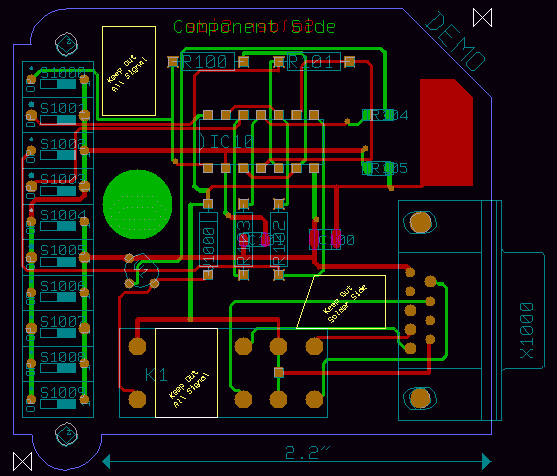
Figure 4-7: Layout after Autorouting
4.6 Special Layout Features
This section describes advanced features and special functions provided with the BAE PCB design system.
4.6.1 Batch Design Rule Check, Report
The
function from the Layout Editor
menu is used to run a complete design rule check on the currently loaded layout. It is strongly recommended to use
before generating CAM data and/or passing CAM data to the PCB manufacturer to avoid design rule violations such as short-circuits, unrouted nets or clearance violations. Use the following commands to perform a batch design rule check on the currently loaded layout
board of the
demo.ddb DDB file:
| Utilities | |
| Batch DRC | |
| Please confirm (Y/N) ? | y |
After performing the design rule check, the
function implicitly activates the
function from the
menu to display the checking results and the design state. The
function can also be called explicitly using the following commands:
| Utilities | |
| Report | |
The following listing is displayed by the
function or after
(zero error lines might be omitted):
File : demo.ddb
Type : Layout / Element : board


Number of Nets .................: 22
Number of Open Connections .....: 0
Number of Short Circuits .......: 0
Copper Distance Violations .....: 0
Documentary Distance Violations : 0
Number of Power Layer Errors ...: 0
Number of Missing Parts ........: 0
Number of Wrong Type Parts .....: 0
Number of Missing Netlist Pins .: 0
Height Distance Violations .....: 0
Power Layers in Use.............: -
Signal Layers in Use............: 1-2
The
Number of Nets report entry displays number of nets defined in the net list of the currently loaded layout. The
Number of Open Connections entry denotes the number of not yet routed (two-point) connections on the currently loaded layout. The
Number of Short Circuits entry denotes the number of short-circuits encountered by the Design Rule Check. The
Copper Distance Violations entry denotes the number of copper layer clearance distance violations online-encountered by the Design Rule Check on the currently loaded element. The
Documentary Distance Violations entry denotes the number of clearance distance violations on documentary layers. The
Number of Power Layer Errors entry denotes number of copper area cross-intersections on split power planes. The
Number of Missing Parts report entry denotes the number of net list parts not yet placed on the currently loaded layout. The
Number of Wrong Type Parts report entry denotes the number of net list parts placed with a wrong part package type (macro) on the currently loaded layout. The
Number of Missing Netlist Pins entry denotes the number of unplaced and/or missing net list pins. Missing net list pins can cause an erroneous open connections count. An indicator is added to the open connections count if net list pins are missing. The
checklnl User Language program can be used to track missing net list pins.
The
Height Distance Violations entry denotes the number of (part) height design rule violations.
The
Power Layers in Use and
Signal Layers in Use report entries display the used power and signal layers. Signal layer 1 to top layer are always assumed to be in use. These entries help to identify power layers without global net assignment, hence with split power planes to be considered by connectivity.
DRC Error Display
The
dialog from the Layout Editor
menu provides the
parameter for selecting DRC distance and height rule violation error display modes and/or colors. The
option displays error boxes using the error color selected with the
function, the default of which is white. The
setting displays error rectangles using the color selected for the layer on which the erroneous element is placed. Errors on layers which are faded-out through
are not displayed.
The
Layout Editor
menu provides the
function for displaying the DRC distance and height rule violation error lists. The DRC errors are listed in a popup menu, indicating error type, error layer and error coordinates for each error. A
to the error position ist triggered when selecting an error from the list using the left mouse button. The
+ and
- keys can be used to move the zoom window through the error position list in either direction.
Note that the modified
BAE HighEnd data structure for storing the layout connectivity data allows for a selective shortcut display, i.e., shortcuts between two nets are displayed by highlighting only those elements causing the shortcut, whilst
BAE Professional highlights the whole connection tree affected by the short-circuit.
Hit the spacebar to return to the
Layout Editor menu.
4.6.2 Color Setup, Color Tables, Pick Preference Layer
The
function from the
menu activates a popup menu for modifying the current color settings. This color setup menu simultaneously can be utilized for displaying the current color assignments. Changing some item-specific color is accomplished by selecting the desired display item using the left mouse button and then selecting the desired color button from the
function. In the layout system,
provides a feature for fast display item fade-out/fade-in. Activating and/or deactivating some item-specific display is accomplished by selecting the desired display item entry with the right mouse button which works as a toggle between fade-out and fade-in. The system won't loose information on currently defined colors of faded-out display items; strike-through color buttons are used for notifying currently faded-out display items.
At overlaps of different elements the resulting mixed color is displayed. The highlight color is also mixed with the color of the element to be marked, thus resulting in a brighter display of that element.
The
function from the
menu is used to save the current color settings with a user-specified name to the
ged.dat system file in the BAE programs directory. When starting the
Layout Editor (or any other layout program module), the color table named
standard is automatically loaded. Any other color table available in
ged.dat can be loaded using the
function from the
menu.
It is a good idea to define color tables for certain tasks such as
stackdef for padstack editing (i.e., with drill holes and drill plan visible) or
unroutes for fast open connections recognition (i.e., with airlines visible only). At the definition of color tables it is to be considered that screen redraw functions will take longer if more objects must be displayed. It is recommended to define task-specific color tables to display only those objects which are important for the corresponding task.
The
function is usually used to allow selection on a specific layer. It also has the useful hidden function of loading a layer-specific color table. These color tables have specific names, and if they don't exist there will be no change in the color display. See
table 4-3 for the color table names assigned to the pick preference layers
(<n> is the layer number, respectively).
Table 4-3 also lists short layer names which can optionally be used in certain layer menus for selecting layers via keyboard input.
Table 4-3: Pick Preference Layer Color Tables and Short Layer Names
| Layer | Pick Preference Layer
Color Table Name | Short
Layer Name |
|---|
| Signal Layer <n> | layer_<n> | <n> |
| Signal Layer All Layers | layer_all | a |
| Signal Layer Middle Layers | layer_def | m |
| Signal Layer Top Layer | layer_def | |
| Power Layer <n> | | p<n> |
| Documentary Layer <n> Side 1 | layer_d<n>_1 | d<n>s1 |
| Documentary Layer <n> Side 2 | layer_d<n>_2 | d<n>s2 |
| Documentary Layer <n> Both Sides | layer_d<n>_a | d<n>sa |
| Board Outline | | b |
| Airlines | | u |
When selecting a certain pick preference layer (e.g., signal layer 2) using the
function, the color table with the corresponding name (e.g.,
layer_s2) is automatically loaded if available in
ged.dat. This feature is most useful for e.g., manual routing.
4.6.3 Layout Net List Changes
The Layout Editor provides functions for performing pin/gate swaps to simplify the routing problem. Alternate package types can be assigned to layout parts, and net list part names can be changed for better legibility of the insertion plan (for manual insertion). These modifications are net list changes which must be backward annotated to the schematics using the
function from the
Schematic Editor (see also
chapter 3.3).
In this section we will apply some pin/gate swaps and change a couple of part names. First of all, use the following commands to set the coordinate display mode to inch and apply group functions to delete all traces from the currently loaded layout:
| Settings | |
| Coordinate Display | |
| Display Inch | |
| Groups | |
| Group Polygon | |
| Traces | |
| Select | |
| Move to [0.1",0.1"] | |
| Move to [2.8",0.1"] | |
| Move to [2.8",2.7"] | |
| Move to [0.1",2.7"] | |
| Done | |
| Delete Group | |
The
function from the
menu is used to perform manual pin/gate swaps. Use the following commands to swap the pins
1 and
2 of the switches named
s1000,
s1001,
s1002 and
s1003, respectively:
| Parts | |
| Pin/Gate Swap | |
| Move to "s1000.1",[0.2",2.3"] | |
| Move to "s1000.2",[0.5",2.3"] | |
| Pin/Gate Swap | |
| Move to "s1001.1",[0.2",2.1"] | |
| Move to "s1001.2",[0.5",2.1"] | |
| Pin/Gate Swap | |
| Move to "s1002.1",[0.2",1.9"] | |
| Move to "s1002.2",[0.5",1.9"] | |
| Pin/Gate Swap | |
| Move to "s1003.1",[0.2",1.7"] | |
| Move to "s1003.2",[0.5",1.7"] | |
Note how the
function provides graphical pin/gate swap indicators. A circle (0.6mm diameter,
color) is displayed for every pin/gate swap enabled pin when the
function is activated. The indicator for the first selected pin turns into a filled square, leaving only swappable pins marked by circles and character codes for the possible swap operations. The character codes are
P for pin swap,
G for gate swap and
A (Array) for gate group swap. Selecting black for the
color deactivates the pin/gate swap indicator display.
Each pin/gate swap is performed using the corresponding pin/gate swap definition from the Logical Library (see also
chapter 7.11 for a description of the
loglib utility program and
chapter 3.2 for a description of the
Packager program module). The following error message is issued if no swap is allowed for the selected pins and/or gates:
Not allowed to swap these pins!
Use the following commands to swap the gates (1,2,3) and (5,6,4) as well as the pins
12 and
13 of the part named
IC10:
| Parts | |
| Pin/Gate Swap | |
| Move to "ic10.(1,2,3)",[1.4",1.8"] | |
| Move to "ic10.(5,6,4)",[1.5",1.8"] | |
| Pin/Gate Swap | |
| Move to "ic10.12",[1.4",2.1"] | |
| Move to "ic10.13",[1.3",2.1"] | |
Use the following commands to perform a part swap for the resistor parts named
R101 and
R103 (this is allowed because the same attribute values are assigned to these parts):
| Parts | |
| Pin/Gate Swap | |
| Move to "r101",[1.6",2.4"] | |
| Move to "r103",[1.4",1.2"] | |
The
function from the Parts menu is used to change part names in the net list. Use the following commands to change the net list part name of connector
X1000 to
filenameX1, and also change the net list part name of diode
V1000 to
V2:
| Parts | |
| Netlist Part Name | |
| Move to "x1000",[2.4",1.5"] | |
| Part Name (X1000) ? | X1 |
| Netlist Part Name | |
| Move to "v1000",[1.2",1.2"] | |
| Part Name (V1000) ? | V2 |
The
function issues the following error message if you try to assign a part name which is already in use for another part:
Part name already in use!
Use the following commands to apply the
function to change the name of part
IC10 to
IC1:
| Parts | |
| Change Part Name | |
| Move to "ic10",[1.2",1.8"] | |
| Part Name (IC10) ? | IC1 |
The airlines previously connected to
IC10 have been disappeared from
IC1. I.e., the
function not only performs a part name change, but also replaces the selected part. With the commands above the part named
IC10 has been replaced with the part
IC1 which is not defined in the net list. Use the following commands to reset this part name change and apply the
function to change the net list part name to
IC1 (note how the airlines connected to
IC1 will appear again):
| Parts | |
| Change Part Name | |
| Move to "ic1",[1.2",1.8"] | |
| Part Name (IC1) ? | ic10 |
| Netlist Part Name | |
| Move to "ic10",[1.2",1.8"] | |
| Part Name (IC10) ? | ic1 |
It is recommended to use the
function with caution. Multiple misuse of the
function can cause short circuits on routed layouts, and it might get very laborious to backtrack part name changes for design corrections.
The layout net list changes accomplished with the previous operations must be backannotated to the schematics and the logical net list. Use the following commands to save the currently loaded layout and return to the BAE main menu:
| File | |
| Save Element | |
| File | |
| Main Menu | |
The BAE main menu is activated. Use the following commands to switch to the
Schematic Editor and run
to transfer the physical net list named
board in in
demo.ddb back to the schematics:
| Schematic | |
| Utilities | |
| Backannotation | |
| Design File Name ? | demo |
| Layout Element Name ? | board |
displays the following messages:
==============================
BARTELS BACKANNOTATION UTILITY
==============================


Design File Name ........: 'demo'
Layout Element Name .....: 'board'
No error occurred!
The
No error occurred! message means that
has been successfully completed, and the logical net list in project file
demo.ddb has been annotated with the physical net list named
board. Hit any key to return to the
Schematic Editor main menu and use the following commands to load the SCM sheet
sheet1 from DDB file
demo.ddb:
| File | |
| Load | |
| Sheet | |
| File Name ? | demo |
| Element Name ? | sheet1 |
You can now examine the currently loaded SCM sheet for modifications introduced by
. Particularly note the part name changes
(IC1 instead of
IC10,
V2 instead of
V1000, etc.) and the pin assignment changes (e.g., at the gates of
IC1 or at the switches
S1000 through
S1003).
4.6.4 SCM Changes, Redesign
Bartels AutoEngineer provides features for modifying SCM sheets of an already completed design, without the need to prepare a completely new layout. This section describes how perform a redesign by making changes to the currently loaded SCM sheet.
Use the following commands to change the
$plname attribute value of the resistor
R104 from
minimelf to
chip1206:
| Symbols | |
| Assign Value | |
| Move to "r104",[210,130] | |
| $plname | |
| Attribute Value ? | chip1206 |
| Return | |
With the commands above the package type assignment for the resistor part
R104 has been changed. Use the following commands to assign value
so14 to the
$plname attribute of each gate of part
IC1, thus defining a non-default package type for
IC1 (the default package type was
dil14):
| Symbols | |
| Assign Value | |
| Move to "ic1.5",[60,110] | |
| $plname | |
| Attribute Value ? | so14 |
| Assign Value | |
| Move to "ic1.1",[100,110] | |
| $plname | |
| Attribute Value ? | so14 |
| Assign Value | |
| Move to "ic1.8",[140,110] | |
| $plname | |
| Attribute Value ? | so14 |
| Assign Value | |
| Move to "ic1.13",[180,110] | |
| $plname | |
| Attribute Value ? | so14 |
Use the following commands to save the currently loaded SCM sheet and load
sheet2:
| File | |
| Save | |
| Load | |
| Sheet | |
| File Name ? | |
| Element Name ? | sheet2 |
The currently loaded SCM sheet contains some
Autorouter control parameter settings (net attribute assignments), which should be modified. Use the following commands to change the
ROUTWIDTH net attribute of
NET from 0.5mm to 0.3mm, change the
ROUTWIDTH attribute of net
Vss from 0.6mm to 0.45mm and change the
MINDIST attribute for net
Vdd from 0.4mm to 0.3mm:
| Symbols | |
| Assign Value | |
| Move to "NET"/Routwidth Symbol | |
| $val | |
| Attribute Value ? | 0.3 |
| Assign Value | |
| Move to "Vss"/Routwidth Symbol | |
| $val | |
| Attribute Value ? | 0.45 |
| Assign Value | |
| Move to "Vdd"/Mindist Symbol | |
| $val | |
| Attribute Value ? | 0.3 |
Use the following commands to return to the BAE main menu (the currently loaded SCM element is automatically saved):
| File | |
| Main Menu | |
Now the BAE main menu is activated. Use the following commands to run the
Packager to transfer the SCM changes to the layout, i.e., to the physical net list named
board (the
demo.ddb job file can be used as design library since it contains all of the information required for packaging):
| Packager | |
| Design File Name ? | demo |
| Design Library Name ? | demo |
| Layout Element Name ? | board |
The
Packager issues the
No error occurred! message after successfully completing the forward annotation to the layout. Hit any key to return to the BAE main menu and use the following command to start the
Layout Editor:
| Layout | |
Now the
Layout Editor is activated. Use the following commands to load the annotated layout:
| File | |
| Load Element | |
| Layout | |
| File Name ? | demo |
| Element Name ? | board |
A connectivity generation is accomplished after loading the layout. Note that there are no airlines connected anymore to the parts
IC1 and
R104, since the package types have been changed for these parts. Use the following commands to delete all parts with changed package type assignments introduced by net list modifications:
| Parts | |
| Delete Update | |
| Please confirm (Y/N) ? | y |
The confirm prompt is only activated if there are parts placed with wrong package types. The
function can be used for checking the layout for wrong package types (simply type
n to the confirm prompt if you want to abort the
function). The
call from above deletes the parts
R104 and
IC1 from the layout and issues the following message:
2 Parts deleted!
Use the following commands to place the previously deleted parts with correct package types:
| Parts | |
| Add Part | |
| Part Name ? | ic1 |
| Jump Absolute | |
| Absolute X Coordinate (mm/") ? | 1.6" |
| Absolute X Coordinate (mm/") ? | 2.0" |
| Place Next Part | |
| Mirror On | |
| Rotate Right | |
| Jump Absolute | |
| Absolute X Coordinate (mm/") ? | 0.35" |
| Absolute Y Coordinate (mm/") ? | 2.0" |
Now all parts are placed again on the layout. You can check this with the
function which should issue the
All parts have been placed already! message.
4.6.5 Defining and Editing Power Layers
The
Bartels AutoEngineer layout system provides features for defining power layers and/or power planes. Use the following commands to define a power layer for signal
Vss:
| Settings | |
| Set Power Layers | |
| 1: --- | |
| Net Name ? | vss |
| End | |
Note how the above-mentioned power layer definition removes the airlines connected to the drilled pins of signal
Vss. Drilled pins are automatically connected to the corresponding power layer (i.e., the
CAM Processor will later generate heat traps at the drillings of power layer pins). The airlines connected to the SMD pins of signal
Vss won't be deleted, i.e., the
Autorouter will automatically connect these pins to the power layer using vias.
Power layer definitions can be displayed in the BAE layout system. Use the following commands to set the color for power layer 1 to dark blue:
| Change Colors | |
| Power 1 | |
| Move to Desired Color, dark blue | |
| Exit | |
On the display of drilled pin definitions there is a distinction whether the pin is connected to a power layer or not. Power layer connections are displayed as circle outlines; isolations, i.e., drills which are not to be connected to any power layer, are displayed as filled circles.
The layer selection menus of the
function from the
menu allow for the selection of power layers. Power planes or isolated areas (net name
-) can be placed on power layers to perform split power plane editing, i.e., to define more than one signal on a single power layer. Power planes are displayed with their outlines which will later be interpreted as isolation line by the
CAM Processor (see also
chapter 4.7.6 of this manual). There is a restriction that no power plane can overlap any other power plane partially since this would cause an ambiguity in the power plane tree detection algorithms. Partial power plane overlaps will cause the design rule check to issue power layer errors; the number of power plane errors detected by the DRC is shown with the
Power Layer Errors entry of the
function. Power planes completely enclosed by other power planes are allowed; the power plane tree detection will always match the "innermost" power plane for connecting.
The layer selection menus of the
function from the
menu allow for the selection of power layers. Text can be placed on power layers to add documentary information to the power layers. When placing text on power layers, the design rule check will perform distance checking against the
and
signal layers. Power layer text is visible on the PCB only if the corresponding power layer is configured as board outside layer (i.e., as either solder side or component side layer). Usually power layers are defined as board inside layers of a multilayer design. Text placed on power layers can serve as control information (e.g., for the layout designer or as plot or film archive information).
4.6.6 Autorouter Via Keepout Areas
There is often the need to define areas where the
Autorouter is allowed to rout traces but must not place vias (e.g., underneath special parts). Via keepout areas can be defined on a routing layer which is not required for the real layout. This "via keepout layer" should then be prohibited with the
Autorouter layer assignment. The
Autorouter considers all objects placed on prohibited layers, and vias and/or via drill holes are assumed to be defined on all layers. I.e., the
Autorouter refrains from placing vias at positions where via pads would intersect with keepout areas on prohibited routing layers.
Use the following commands to place a keepout area on layer 3 matching the region underneath the switches
s1000 through
s1009:
| Areas | |
| Add Keep Out Area | |
| Layer 3 | |
| Move to [0.25",0.4"] | |
| Move to [0.45",0.4"] | |
| Move to [0.45",2.4"] | |
| Move to [0.25",2.4"] | |
| Done | |
Use the following commands to start the
Autorouter (the currently loaded layout will automatically be saved):
| File | |
| Autorouter | |
Use the following commands to define routing layer 3 to be prohibited and start the
(the
Autorouter options such as routing grid, trace width, clearance, etc., have already been defined with the previous
Autorouter session):
| Options | |
| Layer Assignment | |
| Select Layer Number ? | 3 |
| Select Layer Type (P/H/V/A/-) ? | p |
| Select Layer Number ? | |
| Autorouter | |
| Full Autorouter | |
The
will a find 100% routing solution with no vias placed inside the via keepout area. Note also how the SMD pins of the previously defined power layer
Vss (see above) are automatically connected using short traces with vias.
Use the following command to return to the
Layout Editor after successfully completing the autorouting:
| File | |
| Layout Editor | |
4.6.7 Area Mirror Mode
The
function from the
Layout Editor
menu is used to set special display attributes for selectable areas. The
option is the default display mode for any area.
defines the selected area to be always visible. The
option defines the selected area to be visible only when unmirrored (i.e., when placed on the component side). The
option defines the selected area to be visible only when mirrored (i.e., when placed on the solder side). The
function can be used on part, padstack and pad level. It is possible to define SMD parts with differently shaped pads or keepout areas depending on which side of the board the part is placed (for supporting different soldering processes on solder and/or component side).
Use the following commands to load the pad symbol
p1206 from the
demo.ddb DDB file:
| File | |
| Load Element | |
| Pad | |
| File Name ? | demo |
| Element Name ? | p1206 |
There is finger-shaped contact area defined on the currently loaded
p1206 pad. Use the following commands to define this copper area to be visible only when unmirrored (i.e., when placed on the component side):
| Areas | |
| Mirror Display | |
| Move to Area Edge | |
| Visible unmirrored | |
Now the component side pad shape is defined. Use the following commands to define a rectangle-shaped passive copper area to be visible only when mirrored (i.e., when placed on the solder side):
| Areas | |
| Add Passive Copper | |
| Jump Absolute | |
| Absolute X Coordinate (mm/") ? | 0.6 |
| Absolute Y Coordinate (mm/") ? | 0.9 |
| Jump Relative | |
| Relative X Coordinate (mm/") ? | -1.2 |
| Relative Y Coordinate (mm/") ? | 0 |
| Jump Relative | |
| Relative X Coordinate (mm/") ? | 0 |
| Relative Y Coordinate (mm/") ? | -1.8 |
| Jump Relative | |
| Relative X Coordinate (mm/") ? | 1.2 |
| Relative Y Coordinate (mm/") ? | 0 |
| Done | |
| Areas | |
| Mirror Display | |
| Move to Area Corner/Edge | |
| Visible mirrored | |
Use the following commands to save the currently loaded pad symbol and re-load the layout:
| File | |
| Save Element | |
| Load Element | |
| Layout | |
| File Name ? | |
| Element Name ? | board |
The system accomplishes a connectivity generation to correlate the library modifications with the current net list definition. The
p1206 pad is used on the
s1206 padstack symbol, which, in turn, is used on the
chip1206 part symbol. Note how the layout system uses different pad shapes for the mirrored parts
R104 and
C101 and for the unmirrored part
R105.
The
function can be applied on any copper, keepout or documentary polygon defined on a library element which can be mirrored. You can also use this feature to define part keepout areas on documentary layers to perform different part clearance checks depending on which side of the board the parts are placed.
Reflow-Reflow SMT/SMD Soldering Support
A control for setting the
parameter is provided in the
dialog from the
menu to support reflow-reflow SMD/SMT soldering techniques. On default, the
parameter is activated, and polygons with the
, attribute are only visible when not mirrored, whilst polygons with the
attribute are only visible when mirrored. However, with the
, parameter deactivated, all polygons declared as
, are always visible, and all polygons declared as
, are never visible, independently of any (part) mirroring.
, deactivation allows for SMD libraries designed for conventional SMD soldering to be re-used for reflow-reflow SMD soldering.
4.6.8 Automatic Copper Fill
The BAE layout system provides powerful automatic copper fill functions with user-definable minimum structure size and isolation distance. The copper fill algorithm support isolated copper area elimination and automatic heat trap generation with adjustable connection widths and heat-trap-specific isolation distances.
The copper fill functions are available through the
submenu of the Layout Editor
menu.
Copper Fill Parameters
Depending on the current BAE menu setup, copper fill parameters can either be set from the
dialog of the
submenu or through dedicated menu functions in that same menu.
The
function is used to set the copper fill isolation distance parameter for the copper fill algorithm (default 0.3mm). The copper fill clearance distance is applied on default unless some net-specific minimum distance settings are defined through
MINDIST net attributes (see
chapter 7.11). Net-specific minimum distance attribute settings are considered individually.
The
function is used to define the minimum structure size for area generation (default 0.1mm). This value should correspond with the smallest Gerber aperture size to ensure valid Gerber photoplot data generation without overdraw errors.
The
option of the
function causes the copper fill algorithm to generate arc-shaped concave area borders during trace segment isolation; on default octagonal circle interpolation is applied (option
).
The
option of the
function switches off isolated copper area recognition (i.e., the copper washes over the pad that it is to connect to); on default, isolated copper areas are automatically eliminated during active copper generation (option
).
The
option keeps isolated areas and automatically selects them to the current group as they are created.
The
options also support for different processing modes for pins and vias. It is possible to decide whether heat-trap connections should be generated for both pins and vias (option
), for pins only (option
), for vias only (option
), or if direct connections only should be generated (option
).
The
option of the
function deactivates automatic heat trap generation when filling active copper. The default
option
is used to activate automatic heat trap generation, i.e., to create thermal relieves for copper area connections. With
selected, the system prompts for the heat-trap junction width and an optional heat-trap-specific clearance distance, where invalid inputs won't change current settings. On default, the heat trap junction width is set to 0.3mm and the heat-trap clearance is set to zero (i.e., heat-traps are isolated using standard minimum clearance settings).
BAE HighEnd provides the
option for specifying the maximum heat-trap connections count (1, 2, 3 or 4). The default heat-trap generation sequence is left, right, bottom, top.
Copper Fill Workarea Definition
Copper fill workareas are required for copper fill functions to operate. Use the following
Layout Editor commands to define a rectangle-shaped copper fill workarea on layer 1 for the signal named
net:
| Areas | |
| Add Cop.-Fill Area | |
| Net Name ? | net |
| Layer 1 | |
| Move to [0.6",0.4"] | |
| Move to [1.7",0.4"] | |
| Move to [1.7",1.7"] | |
| Move to [0.6",1.7"] | |
| Done | |
A dash string input
(-) to the net name prompt of the
function creates a copper fill workarea which is not assigned to any net. This feature can be used for generating pure shielding areas.
Passive copper areas with signal net connections (e.g., teardrops created as passive copper) are treated like active copper areas of that net and won't be isolated from copper fill areas of that net.
Automatic Copper Fill
The
,
,
and
functions are used to activate automatic copper fill procedures.
performs automatic copper fill on all copper fill workareas.
deletes copper areas from all copper fill workareas. With
and
, the user is expected to select the desired copper fill workarea.
Use the following commands to set the isolation distance to 0.35mm, specify a minimum structure size of 0.15mm, deactivate the automatic isolated copper area elimination and fill the predefined workarea:
| Areas | |
| Copper Fill | |
| Set Fill Clearance | |
| Copper Clearance Distance ( 0.30mm) ? | 0.35 |
| Min. Fill Size | |
| Min. Fill Structure Size ( 0.10mm) ? | 0.15 |
| Insol. Area Mode | |
| Keep Islands | |
| Fill single area | |
| Move to Copper Fill Workarea | |
The system fills the selected workarea with active copper assigned to the signal named
net and isolated from other signal levels. The copper fill process is very laborious and might last a few moments to complete. You should perform a screen redraw and examine the results after the copper fille procedure is completed. You can reset the copper fill, change the copper fill parameters and re-apply the copper fill function if you are not satisfied with the results (maybe because of either too small or too large structures being generated).
Use the following commands to reset the copper fill from above and re-apply the copper fill with automatic isolated area generation:
| Areas | |
| Copper Fill | |
| Clear single area | |
| Insol. Area Mode | |
| Delete Islands | |
| Fill all areas | |
The minimum structure size (i.e., the smallest area size to be generated with copper fill) has basic meaning for subsequent
CAM Processor. The copper fill algorithm uses the minimum structure size for automatically rounding off convex corners to avoid acute-angled areas. You should specify the minimum structure size according to the size of the smallest round aperture defined for Gerber output to ensure that Gerber photoplot data can be generated without overdraw errors (see also
chapter 4.7 of this manual).
Copper Fill Complexity
The CPU time and memory requirements of the copper fill algorithm strongly depend on the quantity and complexity of the structures to be isolated and/or generated. Orthogonal structures make the job much easier than e.g., arc-shaped objects since a lot more time consuming geometric distance calculations and complex floating point operations are required for the latter.
Figure 4-8 elucidates how the complexity of the objects to be isolated and particularly their mutual positioning strongly affects memory requirements during copper fill. Note, however, that
figure 4-8 does not show what large amount of temporary data is required for the area reduction and expansion algorithms used for generating correct copper fill areas. Defining more smaller copper fill workareas instead of a few large ones can often be the workaround when running into memory problems using the copper fill function on main memory limited PC systems.
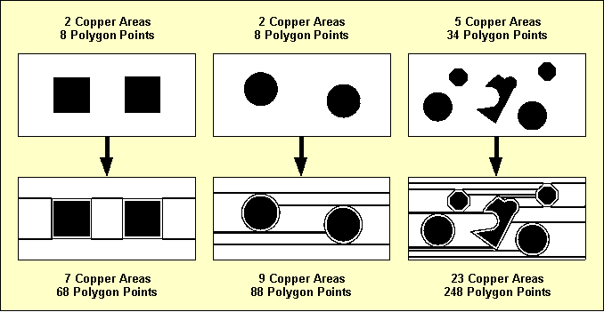
Figure 4-8: Automatic Copper Fill Complexity
You can use one of the
,
and
options instead of the
default option from the
function to reduce the complexity and number of fill areas. This allows for trace corners and/or full circles to be isolated like octagons, thus also reducing the amount of Gerber data if no Gerber arc commands can be used.
To avoid long response times after unintentionally activating the copper fill function, automatic copper fill can be canceled by pressing any key and confirming the abort request with a verification menu. Note, however, that canceling is not possible anymore at the final stage of connectivity generation, and that areas generated before the abort request must be explicitly eliminated using the
function.
Using the copper fill function considerably increases the number of copper areas and polygon points. This raises the CPU time requirements for the
function if the
function type is set to a corner to corner airline calculation (see
chapter 4.3.2 of this manual). In such cases it can be worthwhile to use a pin to pin calculation method to reduce
CPU time requirements. The
from the
Layout Editor
menu is used to set the
function type.
Copper Area Hatching
The
submenu provides the
function for transforming copper areas into line or cross hatched areas with user-definable hatching width and hatching clearance.
Hatching is accomplished through trace segments generation. The width of the produced trace segments can be set with the
function (default 0.3mm) whilst the spacing between produced trace segments can be set with the
function (default 1/20 inch).
The
function is used to designate the hatching type. The default
option generates hatch areas with diagonal trace segments. The
option generates hatch areas with crosswise intersecting diagonal trace segments.
The hatching process is activated by calling the
function and selecting the copper area to be hatched.
Use the following commands to set the coordinate display mode to inch, and transform the circle-shaped copper area on signal layer 2 of the layout to a line-hatched area with a hatching distance of 1mm:
| Settings | |
| Coordinate Display | |
| Display Inch | |
| Areas | |
| Copper Fill | |
| Hatching Distance | |
| Hatching Line Spacing ( 1.27mm) ? | 1 |
| Hatch Copper Area | |
| Move to Passive Copper Area/Signal Layer 2, [0.8",1.8"] | |
Use the following commands to set the hatching width to 0.2mm and transform the active copper area (signal
vdd) on signal layer 1 of the layout into a cross-hatched area:
| Areas | |
| Copper Fill | |
| Hatching Width | |
| Hatching Line Width ( 0.30mm) ? | 0.2 |
| Hatching Mode | |
| Grid Hatching | |
| Hatch Copper Area | |
| Move to Active Copper Area "vdd"/Signal Layer 1, [2.5",2.0"] | |
The
function generates a special layout polygon type called hatched copper area. The hatching and the hatching area outline are generated using traces with a trace width according to the hatching width setting. The traces are strongly connected with the hatched copper polygon to support general
Layout Editor polygon functions such as
or
.
The PCB layout example should now look like the one shown in
figure 4-9 if you correctly executed all operations.
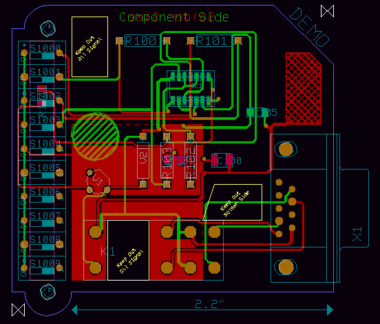
Figure 4-9: Layout with Filled Copper Areas
This might be a good time to save the layout:
| File | |
| Save Element | |
4.6.9 Library Update
The
function is one of the most powerful features of the
Bartels AutoEngineer.
is usually used to update a job-specific library in order to correlate it with the contents of some master library.
Use the following commands to copy the currently loaded layout to the
democopy.ddb DDB file (with default layout element name), and load the copied layout:
| File | |
| Save Element As | |
| File Name ? | democopy |
| Element Name ? | |
| Load Element | |
| Layout | |
| File Name ? | democopy |
| Element Name ? | |
Now the copied layout appears on the screen. However, this layout contains only those objects which are directly defined on the layout. The lower level library elements (parts, padstacks, pads) are not displayed since they have not been copied with the
function to prevent from overwriting existing library elements in the
democopy.ddb destination file. The system will issue either the
Connected pins missing!
message or the
Cannot load all elements (display not complete)!
message in the status line. Use the following commands to correlate the job-specific library of DDB file
democopy.ddb with the contents of DDB source file
demo.ddb:
| File | |
| Update Library | |
| Layout | |
| File Name ? | |
| Element Name ? | |
| Source File Name ? | demo |
After a few moments the system should issue a
Library elements replaced! message which means that all library elements referenced from the currently loaded layout have been copied from the specified library source file. Use the following commands to re-load the layout in order to display the library update
( works on DDB file level, it doesn't affect elements in main memory):
| File | |
| Load Element | |
| Layout | |
| File Name ? | |
| Element Name ? | |
The
function can also be used to correlate the job-specific library with the contents of a different layout library file. Use the following commands to perform a library update for the currently loaded layout using the library source file
demolib.ddb, and re-load the layout (note how the
r04a25 resistor package type is updated with the definition from
demolib.ddb):
| File | |
| Update Library | |
| Layout | |
| File Name ? | |
| Element Name ? | |
| Source File Name ? | demolib |
| Load Element | |
| Layout | |
| File Name ? | |
| Element Name ? | |
The
function is used for substituting selectable library elements with definitions from a certain library source file. Use the following commands to replace the
r04a25 part symbol and the
p1206 pad symbol of the current
democopy.ddb DDB file with the corresponding definitions from the
demo.ddb DDB file, and re-load the layout
( works on DDB file level, it doesn't affect elements in main memory):
| File | |
| Replace Element | |
| Part | |
| File Name ? | |
| Element Name ? | r04a25 |
| Source File Name ? | demo |
| Please confirm (Y/N) ? | y |
| Replace Element | |
| Pad | |
| File Name ? | |
| Element Name ? | p1206 |
| Source File Name ? | demo |
| Please confirm (Y/N) ? | y |
| Load Element | |
| Layout | |
| File Name ? | |
| Element Name ? | |
4.6.10 Back Net List
The
function from the
menu is most useful for certain applications such as high frequency design, where net list data is requested to be automatically generated from the copper located on the PCB.
The mode of operation of this function should be demonstrated using the currently loaded layout from DDB file
democopy.ddb. Delete the trace which connects the pins
NO1 and
4 of the parts named
K1 and
X1, and reset the definition of power layer
vss:
| Traces | |
| Delete Trace | |
| Move to Trace,e.g.[2.35",0.9"] | |
| Settings | |
| Set Power Layers | |
| 1: vss | |
| Net Name ? | - |
| End | |
Note how the deleted trace and power layer definition are replaced with airlines. Use the following commands to add a trace to connect the pins
2 and
1 of the parts named
R100 and
R101:
| Traces | |
| Add Trace | |
| Move to "R100.2",[1.4",2.4"] | |
| Move to "R101.1",[1.6",2.4"] | |
| Done | |
The system now indicates a short-circuit error. Use the following commands to save the layout, run
to generate a net list with the same file and element name, and immediately re-load the layout again
( stores to DDB file without changing the currently loaded net list data):
| File | |
| Save Element | |
| Utilities | |
| Back Netlist | |
| File Name ? | |
| Element Name ? | |
| File | |
| Load Element | |
| Layout | |
| File Name ? | |
| Element Name ? | |
Now the system performs a connectivity generation to correlate the layout with the net list which was previously generated with
. Note that there are no airlines displayed anymore after completing the connectivity generation. The layout does not contain any open connections and/or short-circuits anymore (you can check this with
and
from the
menu). Deleting the trace which was previously causing a short-circuit would now result in an airline display.
Another useful application of the
function net list generation from Gerber data which was previously loaded with the
CAM View module (for more details see
chapter 4.8 of this manual).
4.6.11 Blind and Buried Vias
Blind and buried vias are partial vias which can be used for layer changes when routing multilayer layouts. Routing with blind and buried vias can considerably increase the routability of multilayer layouts with four or more signal layers.
The BAE
Layout Editor features arbitrary pad layer assignment (see also
chapter 4.2.2 for more details on creating padstacks) and drill classes to support the definition of blind and buried vias. Drill classes should be assigned to certain layer-sets to support CAM drill data output for selectable layer-sets (see also
chapter 4.7 for more details on drill data output). There are no system-imposed restrictions on how to define and/or assign drill classes. You can, e.g., use drill class
A for layer-set 1-2, drill class
B for layer-set 2-3, drill class
C for layer-set 3-4, etc. Note, however, that the drill class assignment must be considered for correct drill data output by the
CAM Processor, and that the layout top layer setting (see also
chapter 4.3.1) gains special meaning when using blind and buried vias.
A typical configuration for 4-layer layouts is the definition of the vias
via (for all layers),
via_12 (for layer-set 1-2),
via_23 (for layer-set 2-3) and
via_34 (for layer-set 3-4). All these vias are simultaneously available for routing when selected to the via list (see also
chapter 4.3.4 for details on how to select vias)
The
Layout Editor command used during interactive routing automatically selects the via with the least possible layer occupancy. The same principle is applied by the
Autorouter. At least one via for all signal layers required for autorouting. Additionally, the
Autorouter can e.g., simultaneously use vias for the layer-sets 1-2-3, 1-2, 2-3, etc. However, to avoid backtracking ambiguities, the
Autorouter is restricted in that it can not use vias with multiple mutually intersecting layers. I.e., the
Autorouter refuses to use a via for layer-set 1-2-3 and another via for layer-set 2-3-4 at the same time (error message
Invalid via padstack (cannot use it)!).
Using the
CAM Processor for generating drill data output for the drill holes defined on partial vias requires corresponding drill class(es) to be specified.
The production of PCBs with blind and buried vias is usually more expensive than the production of standard multilayer boards. However, using blind and buried vias increases the routability of multilayer layouts and also supports advanced PCB manufacturing technologies such as plasma-etched via production processes.
4.6.12 Exiting the Layout System
Don't forget to save the currently edited layout element before exiting the
Layout Editor:
| File | |
| Save Element | |
Returning to Main Menu
The following commands can be used from each program module of the BAE layout system (except for the
Autorouter) to return to the BAE Main Menu (BAE Shell):
| File | |
| Main Menu | |
The
function automatically saves the currently loaded layout element. From the BAE Shell, the following command can be used to return to the operating system:
| Exit BAE | |
Exiting BAE
The following commands can be used from each program module of the BAE layout system to return to the operating system, i.e., to exit the
Bartels AutoEngineer:
| File | |
| Exit BAE | |
The
function activates a confirmation request if the currently loaded element has not yet been saved. In this case you should abort the
function, save the current element, and then call
again, as in:
| File | |
| Exit BAE | |
| Please confirm (Y/N) ? | n |
| File | |
| Save Element | |
| File | |
| Exit BAE | |
4.7 CAM Processor
4.7.1 Starting the CAM Processor
Before starting the
CAM Processor for generating real project manufacturing data, you should always perform a complete design rule check using the
function from the Layout Editor
menu. Subsequently the DRC result should be examined with the
function. It is strongly recommended to refrain from generating and/or releasing any
CAM Processor output if clearance violations, short circuits or open connections are indicated since this will (almost certainly) result in the production of faulty PCBs.
It is recommended to start the
Bartels AutoEngineer from in the directory where the design files should be generated since this considerably simplifies job file access. If you intend to process the examples provided with this manual it is recommended to move to the BAE examples directory installed with the BAE software. The
Layout Editor can be called from the
Bartels AutoEngineer main shell. Start the BAE shell by typing the following command to the operating system prompt:
> bae
Move the menu cursor to the Layout menu item and confirm this choice by pressing the left mouse button:
| Layout | |
Now the
Layout Editor program module is loaded and the
Layout Editor menu is activated. If this fails to happen then check your BAE software installation (see the
Bartels AutoEngineer® Installation Guide for details on how to perform a correct installation).
Use the
command from the Layout Editor
menu to call the
CAM Processor:
| File | |
| CAM Processor | |
If a layout element was previously processed in the
Layout Editor, then this element will automatically be saved and re-loaded to the
CAM Processor. Within the
CAM Processor the
function from the
menu is used to load layout elements of any hierarchy level. Use the following commands to load the layout named
board from DDB file
demo.ddb:
| File | |
| Load Element | |
| Layout | |
| File Name ? | demo |
| Element Name ? | board |
The system issues the
Cannot load character font! error message, if the font used in the loaded element is not available in the
ged.fnt font file from the BAE programs directory.
Without character font data, the
CAM Processor fails to plot any text defined on the currently loaded layout element. You should either supply the requested character font (e.g., use the
fontconv utility program) or assign an existing font to the layout element using the
function from the Layout Editor
menu before producing any CAM output.
4.7.2 CAM Processor Main Menu
The
CAM Processor standard/sidemenu user interface provides a menu area on the right side, consisting of the main menu on top and the currently active menu below that main menu. After entering the
CAM Processor the
menu is active and the menu cursor points to the
function.
The Windows and Motif versions of the
CAM Processor can optionally be operated with a pull-down menu user interface providing a horizontally arranged main menu bar on top. The
WINMENUMODE command of the
bsetup utility program is used to switch between
SIDEMENU and
PULLDOWN Windows/Motif menu configurations (see
chapter 7.2 for more details).
The following main menu is always available whilst processing layout data with the
CAM Processor:
Display
The
or
menu can either be activated by selecting the corresponding main menu item or by pressing the middle mouse button. The
or
menu provides useful functions for changing display options such as zoom window, zoom scale, input grid, color settings, etc.
Control Plot
The
menu provides the functions for generating HP-GL pen plots, PCL HP-laser prints and Postscript output.
Gerber Photoplot
The
menu provides the functions for generating Gerber photo plots, also including facilities for defining and managing Gerber aperture tables.
Drilling+Insertion
The
menu provides the functions for generating drill data output (format Sieb&Meier and/or Excellon ) and insertion data output (generic format).
Plot Parameters
The
menu is used to set general plot parameters (plot tolerance, CAM origin, CAM rotation, CAM mirror mode) and to define special parameters for generating negative power layer plots. The
menu also provides features for controlling the processing of special layers such as the
,
,
and
layers.
Utilities
The
menu provides functions for exiting BAE, returning to the BAE main shell, calling the
Layout Editor and starting
User Language programs. The
menu can also be used for loading layout elements, listing DDB file contents, setting the display grid and the coordinate display mode, or removing error markers.
4.7.3 Customized CAM Processor User Interface
Menu Assignments and Key Bindings
The BAE software comes with User Language programs for activating a modified
CAM Processor user interface with many additional functions (startups, toolbars, menu assignments, key bindings, etc.). The
bae_st User Language program is automatically started when entering the
CAM Processor.
bae_st calls the
uifsetup User Language program which activates predefined
CAM Processor menu assignments and key bindings. Menu assignments and key bindings can be changed by modifiying and re-compiling the
uifsetup source code. The
hlpkeys User Language program is used to list the current key bindings. With the predefined menu assignments of
uifsetup activated,
hlpkeys can be called from the
function of the
menu. Menu assignments and key bindings can be listed with the
uifdump User Language program. The
uifreset User Language program can be used to reset all currently defined menu assignments and key bindings.
uifsetup,
uifdump and
uifreset can also be called from the menu of the
keyprog User Language program which provides additional facilities for online key programming and
User Language program help info management.
Cascading Windows/Motif Pulldown Menus
The Windows and Motif pulldown menu user interfaces of the
CAM Processor provide facilities for cascading submenu definitions. I.e., submenus can be attached to other menu items. The
uifsetup User Language program configures cascading submenus for the pulldown menu interfaces of the Windows/Motif
CAM Processor modules. This allows for easy submenu function location (and activation) without having to activate (and probably cancel) submenus. The function repeat facility provided through the right mouse button supports cascading menus to simplify repeated submenu function calls.
Windows/Motif Parameter Setup Dialogs
The following Windows/Motif parameter setup dialogs are implemented for the
CAM Processor:
- - : General CAM/Plot Parameters
- - : Display Parameters
- - : Control Plot Parameters
- - : Gerber Photoplot Parameters
- - : Drilling Data Output Parameters
The
uifsetup User Language program replaces the parameter setup functions of the Windows and Motif pulldown menus with the above menu functions for activating the corresponding parameter setup dialogs.
Windows/Motif Pulldown Menu Konfiguration
When using pulldown menus under Windows and Motif, the
uifsetup User Language program configures the following modified
CAM Processor main menu with a series of additional functions and features:
4.7.4 In-built CAM Processor System Features
Automatic Parameter Backup
The
CAM Processor provides an in-built feature for automatically saving important operational and plot parameters with the currently processed layout and/or part symbol. The following parameters are stored to the current design file when changing to the BAE main menu or to the
Layout Editor (i.e., CAM parameter backup can only be suppressed when exiting BAE):
- Name of the currently loaded Layout Color Table
- Input Grid
- Display Grid
- Coordinate Display Mode
- Wide Line Draw Start Width
- Output Mode Board Outline
- Output Mode All Signal Layers
- Output Mode Plot Marker Layer
- Plot/CAM Accuracy/Symbol Tolerance
- Plot/CAM Origin Coordinate
- Plot/CAM Rotation Mode
- Plot/CAM Mirroring Mode
- Power Layer Heat Trap Minimum Distance
- Power Layer Isolation Minimum Distance
- Power Layer Heat Trap Range/Tolerance
- Power Layer Isolation Range/Tolerance
- Power Layer Border Width
- Power Layer Isolation Drawing Width
- Control Plot Output File Name/Device
- Control Plot Scaling Factor
- HP-GL Plot Pen Width/Standard Line Width
- HP-GL Plot Speed
- HP-GL Plot Filling Mode
- Gerber Output File Name/Device
- Gerber Aperture Table Name
- Gerber Format/Plotter Units
- Gerber Standard Line Width
- Gerber Fill Mode
- Gerber Arc Plotting Mode
- Drilling Data Output File Name/Device
- Drilling Tool Table Output File Name/Device
- Drilling Tool Tolerance/Accuracy
- Insertion Data Output File Name/Device
Parameter sets are stored with special names according to the currently processed layout database hierarchy level. The layout element name is used for layout elements, parameter set name
[part] is used for layout part symbol elements,
[padstack] is used for layout padstack elements and
[pad] is used for layout pad elements. When loading an element, the corresponding parameter set is automatically loaded as well, thus providing a convenient way of activating a default parameter set suitable for processing the selected design and/or library element type.
Output Device
The
functions from the
and
menus are used to specify the CAM data output device. The output can either be written to a file, or directly to the plotter and/or printer. When plotting to a file, the desired output file name must be specified. When writing directly to the plotter, the name of the output port where the plotter is connected (e.g.,
com2,
lpt1 under DOS) must be specified. Take care that enough disk space is available when writing to a file and that the corresponding interface is correctly initialized when directing output to a hardware device. CAM output aborts with one of the following error message if neither of these requirements are met:
Error creating file!
Error writing ASCII file!
The
CAM Processor will prompt for the output device name after activating the desired output function, if no default plot device has been been specified with the
function. Popup menus for fast output file selection are integrated to the
,
,
,
,
,
,
,
,
,
and
functions of the
,
and
menus. Files ending on
.ass,
.con,
.ddb,
.def,
.exe,
.fre,
.ulc and
.usf are faded out from the output file menus for data security reasons. New output file names can optionally be typed in via keyboard.
User Language
The
Bartels User Language Interpreter is integrated to the
CAM Processor, i.e.,
User Language programs can be called from the
CAM Processor, and it is possible to implement any user-specific
CAM Processor function required such as status display, parameter setup, reports and test functions, special CAD/CAM output and plot functions, customer-specific batch procedures, etc.
The
CAM Processor provides both explicit and implicit
User Language program call facilities.
User Language programs can be started with explicit program name specification using the
function from the
menu (empty string or question-mark
(?) input to the program name query activates a
User Language program selection menu).
User Language programs can also be called by simply pressing special keys of the keyboard. This method of implicit
User Language program call is supported at any time unless another interactive keyboard input request is currently pending. The name of the
User Language program to be called is automatically derived from the pressed key, i.e. pressing a standard and/or function key triggers the activation of a
User Language program with a corresponding name such as
cam_1 for digit key
1,
cam_r for standard key
r,
cam_# for standard key
#,
cam_f1 for function key
F1,
cam_f2 for function key
F2, etc.
The
CAM Processor
User Language Interpreter environment also features event-driven
User Language program calls, where
User Language programs with predefined names are automatically started at certain events and/or operations such as
cam_st at CAM Processor module startup,
cam_load after loading a design element,
cam_save before saving a design element,
cam_tool at the selection of a toolbar item and
cam_zoom at the change of the zoom factor. The module startup
User Language program call method is most useful for automatic system parameter setup as well as for key programming and menu assignments. The element save and load program call methods can be used to save and restore element-specific parameters such as the zoom area, color setup, etc. The toolbar selection event must be used to start
User Language programs which are linked to toolbar elements. The zoom event can be used to apply an update request to a design view management feature.
Bartels User Language also provides system functions for performing key programming, changing menu assignments and defining toolbars. These powerful features can be applied for user interface modifications. Please note that a large number of additional functions included with the
CAM Processor menu are implemented through the
User Language programs delivered with the BAE software.
See the
Bartels User Language Programmer's Guide for a detailed description of the
Bartels User Language (chapter 4.2 lists all
User Language programs provided with the BAE software).
Neural Rule System
A series of advanced
Bartels AutoEngineer features are implemented through the integrated
Neural Rule System. See
chapter 6.3.2 for the rule system applications provided with the
Bartels AutoEngineer. Some of these applications allow for special manufacturing data outputs and for extended control over manufacturing data generation processes.
4.7.5 Plot Parameters
The
CAM Processor supports a series of general parameters for controlling the CAM output such as plot tolerance, CAM rotation, CAM mirror mode, etc. These parameters can be changed using the functions provided with the
menu. It is strongly recommended to set appropriate plot parameters before generating CAM output.
Each input prompt at the specification of plot parameters includes a parentheses-enclosed display of the current parameter value setting. On invalid parameter input values the
CAM Processor issues an error message such as
Invalid numeric value!, and the current parameter value is left unchanged.
Plot Parameter Save/Load
CAM plot parameter settings are automatically stored with the currently processed design file when switching to another BAE module (see above,
chapter 4.7.4). The
CAM Processor
menu also provides the
and
functions.
can be used to save the current CAM plot parameter settings to a different DDB file.
can be used to load CAM parameter settings from a selectable DDB file.
Plot/CAM Origin
The
function is used to set the origin of the output coordinate system. When loading a layout element the CAM origin is automatically set to the lower left corner of that element. When selecting the plot rotate or the plot mirror option (see below), then the CAM origin is automatically moved from the lower left to the upper left corner of the currently loaded element (or vice versa). The
function can be used to set the CAM origin to an arbitrary point inside the element boundaries. It is always possible to avoid negative output coordinates which certain output devices might not be able to understand and/or process.
The plot parameter dialog of the
CAM Processor Windows and Motif versions provides a button for resetting the CAM origin to its default position.
Plot/CAM Rotate
The
function provides the options
and
. The
option sets the 0 degree plot rotation (which is the default). The
option produces a 90 degree counter-clockwise rotated plot output. Negative output coordinates might be produced when rotating plots. Some printers or plotters refuse to process negative coordinates. The
option automatically moves the CAM origin from the lower left to the upper left corner of the element (or vice versa), thus ensuring positive output coordinates only. However,
does not change arbitrary CAM origin settings, i.e., positive output coordinates must then be enforced by replacing the CAM origin manually (see above).
To indicate CAM rotation mode settings, a mirror mode specific example text and an arrow are placed at the CAM origin marker if CAM mirroring and/or rotation is selected.
Plot/CAM Mirror
The
function provides options for mirroring the CAM output:
| Plot Parameters | |
| Plot/CAM Mirror | |
produces output as displayed on the screen.
produces output mirrored at the X-axis crossing the CAM origin.
mirrors all coordinates at the X-axis crossing the CAM origin, except for the texts which are plotted unmirrored.
performs X-axis text mirroring only.
mirrors all coordinates at the X-axis crossing the CAM origin, and additionally performs Y-axis text mirroring.
performs Y-axis text mirroring only.
Figure 4-10 illustrates the effects of the different mirror options.
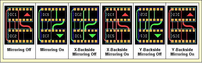
Figure 4-10: CAM Mirror Modes
With all mirror modes, the position of the CAM origin must be considered. With mirroring activated, the CAM origin should be set to the upper left corner of the layout element to ensure positive coordinates output. With the CAM origin set to default,
automatically replaces the CAM origin to produce positive output coordinates only.
To indicate CAM mirror mode settings, a mirror mode specific example text and an arrow are placed at the CAM origin marker if CAM mirroring and/or rotation is selected.
All Layers Mode
The
function is used to designate how objects should be treated, which are placed on signal layers
and
or on both sides of documentary layers. With documentary layers, the
refers to side 1 and side 2 and corresponds with the
options of the documentary layer menus. With signal layers, the
refers to the
and
signal layer selections. With option
, all layer objects are only plotted when selecting the corresponding plot layer
(,
or
with documentary layers). With option
, all layer objects are plotted together with the selected plot layer. I.e., when plotting signal layer 1 with
the objects on signal layer
are also plotted, when plotting
of documentary layer
the objects on
-
are also plotted, etc. On default, the
option is used.
The
plot parameter of the
BAE HighEnd
CAM Processor also provides the
,
and
options. These modes restrict the output of inside layer pin and/or via pads to only those pads which have connections to other elements on the selected inside layer.
plots only connected inside layer pin and via pads.
plots all inside layer pin pads and only connected inside layer via pads.
plots all inside layer via pads and only connected inside layer pin pads. Inside layers are all signal layers except for layer 1 and the signal layer selected with the
function.
Symbol Tolerance
The
function is used to set the plot accuracy for filling areas and/or creating structures using the available set of tools. It allows to plot elements to be smaller by the specified plot tolerance value if this creates more efficient output. E.g., when photoplotting a round pad with 0.062 inch diameter and the plot tolerance set less than 0.002 inch, then the 0.060 inch aperture is used to draw in a circle to produce the correct size; if the tolerance is set greater than 0.002 inch then the 0.060 inch aperture is flashed, since it is smaller than the required size but within the tolerance and much more efficient.
The plot tolerance is only calculated to the inside of the structures to be plotted since, otherwise, short-circuits might be produced. The default plot tolerance value is 0.15mm. For structures which cannot be plotted correctly using the smallest aperture and/or pen width, the
CAM Processor uses the smallest available tool to generate that structure. Such structures produce overdraw plot errors which are reported and/or indicated with highlight. It is strongly recommended to refrain from passing CAM output with overdraw errors to the PCB manufacturer since this could produce PCBs containing short-circuits. The
function from the
menu can be used to reset the overdraw error display.
Board Outline and Plot Markers
The
and
functions are used to designate whether the board outline and/or the plot markers should be plotted together with other layers. With the
option of the
function the board outline can be plotted only when selecting the
plot layer. With the
option, the board outline is plotted together with any other plot layer. With the
option of the
function, the plot markers can be plotted only when selecting the corresponding plot markers documentary layer. With the
option, the plot markers are plotted together with any other plot layer. The plot markers documentary layer can be defined with the
LAYPLTMARKLAY command of the
bsetup utility program (see
chapter 7.2 for more details). On default the
and the
options are used.
4.7.6 Power Layers
When plotting power layers, the
CAM Processor automatically generates negative plots using special power layer plot parameters. Text placed on power layers is plotted using the standard line width or the selected pen width.
When editing power layers, the
Layout Editor obviously does not know about the power plot parameters which will later be set in the
CAM Processor. I.e., the
Layout Editor's DRC cannot perform complete electric checking on power layer plot data generated in the future. It is strongly recommend to perform extensive visual checks on power layer plots before passing such plot data to the film and/or PCB manufacturer (use the
CAM View module). Connectivity-changing isolations might be produced, if the power plot isolation width parameters are set too large.
Power Layer Border
The
function from the
menu is used to define the PCB power layer border width, i.e., the copper-free PCB boundary area to be generated when plotting power layers. The default value for the power layer border width is 2.1mm. If the PCB board outline contains arc-shaped segments, then an appropriate tool (aperture, standard line width or pen) for drawing the board outline with the specified power layer border width is required.
Split Power Planes and Power Plane Isolation
Both active and passive power planes placed on power layers are generated by plotting the power plane outline which then is the isolation line of the power plane. Processing active power planes with specific net assignment generates split power planes, whilst passive power planes without net assignment result in isolated areas on the power layer. The width of the power plane isolation can be adjusted with the
function from the Plot Parameters menu. The default power plane isolation width is 0.3mm.
Power Layer Pin Isolation
Pins not connected to the power layer and/or the power plane net are isolated by placing filled circles at the corresponding pin drill holes. The isolation circle diameters are calculated from the drill hole diameters and the plot parameters to be set with the
and
functions from the
menu. The
function is used to specify the minimum distance between the edge of the drill hole and the outside of the isolation circle placed in the power layer. The default value for the power layer isolation minimum distance is 0.4mm. The
function is used to specify the outward tolerance of the isolation area. The default value for the power layer isolation is 0.5mm. The minimum isolation circle diameter is calculated as in
Drill Diameter + 2 × (P-IS Min. Distance)
The maximum isolation circle diameter is calculated as in
Drill Diameter + 2 × (P-IS Min. Distance) + 2 × (P-IS Tolerance)
Figure 4-11 illustrates the effects of the minimum isolation distance and the isolation tolerance power plot parameter settings.
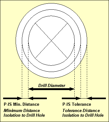
Figure 4-11: CAM Power Layer Isolation
Heat Traps
Pin connections into power layers or to power planes placed on power layers are automatically generated with heat trap construction. A heat trap is constructed with four 45 degree isolation circle segments placed round the drill hole of the pin, thus preventing from too much heat flow. The heat trap circle diameters are calculated from the drill hole diameters and the plot parameters to be set with the
and
functions from the
menu. The
function is used to specify the minimum distance between the edge of the drill hole and the outside of the heat trap circle. The default value for the heat trap minimum distance is 0.4mm. The
function is used to specify the outward tolerance of the heat trap. The default value for the heat trap tolerance is 0.5mm. The heat trap circle diameters are calculated analogously to the isolation circles (see above).
With Gerber photoplot, the
CAM Processor checks if there is a thermal aperture available with a diameter matching the calculated tolerance range, which can be used to flash the heat trap. Otherwise, the heat trap is drawn using the smallest round aperture valid for line strokes.
Use the following commands to set the power layer border width to 0.3mm, the power plane isolation width to 0.25mm, the minimum pin isolation width to 0.35mm with a tolerance of 0.4mm (i.e., maximum pin isolation width 0.75mm) and the heat trap distance to 0.35mm with 0.45 tolerance (i.e. maximum heat trap distance 0.8mm):
| Plot Parameters | |
| Power Layer Border | |
| Power Layer Border Width ( 2.10mm) ? | 0.3 |
| Power Layer Isol. | |
| Power Layer Isolation Width ( 0.30mm) ? | 0.25 |
| P-IS Min. Distance | |
| Min. Distance Isolation to Drill Hole ( 0.40mm) ? | 0.35 |
| P-IS Tolerance | |
| Tolerance Isolation to Drill Hole ( 0.50mm) ? | 0.4 |
| P-HT Min. Distance | |
| Min. Distance Heat Trap to Drill Hole ( 0.40mm) ? | 0.35 |
| P-HT Tolerance | |
| Tolerance Heat Trap to Drill Hole ( 0.50mm) ? | 0.45 |
4.7.7 HP-GL Output
The
function from the
menu is used to produce pen plots in HP-GL (Hewlett-Packard Graphics Language) format.
The
function is used to define the pen width for generating HP-GL output data. Structures smaller than the plotter pen width cannot be drawn without overdraw errors. The default plotter pen width is 0.3mm. Pen width value specifications can range from 0.01mm to 10.0mm.
The
function is used to control the pen plotter speed, i.e., the speed at which the pen can be moved by the HP-GL plotter. The system accepts either
S input for maximum speed or non-negative integer plotter speed values in cm/s units. The default plotter speed corresponds with
S (maximum speed). The maximum speed value specification is 99cm/s.
The HP-GL coordinates are written in plotter units where 40.2 plotter units are 1 millimeter. Some HP-GL "compatible" plotters are based on 40 plotter units per millimeter. The
function can be used to specify a scale factor for producing true to scale output with non-default plotter units. The default plot scale value is 1.0 for true to scale output. Plot scale specifications can range from 0.1 to 100.0.
The
function provides the options
and
.
causes the system to refrain from filling the plot structures, i.e., only outlines are drawn for filled areas. Switching off the fill mode is most useful for fast control plots.
is used to select the default fill mode.
The
function is used to produce HP-GL pen plots. The user is prompted for the plot layer and the pen number (1..99), and for the name of the output file (if no default output device was specified with
). Note the
option provided with the layer selection menu of the
function. This option can be used for writing the plot data of multiple selectable layers to a single output file. With the
option a popup menu is provided for selecting and/or deselecting the plot data output layers using the right mouse button. Layer selections with the left mouse button also allow for layer-specific pen number selections (on default pen 1 is used for each layer). The
button is used to select all currently visible layers for output, with the pen numbers automatically set to modulo eight of the corresponding layer colors.
Use the following commands to set the plotter pen width to 0.2mm, set the plotter speed to 10cm/s, switch off the fill mode and plot the documentary layer
-
of the currently loaded layout to an HP-GL plot file named
demo_bs2.plt using pen number 1:
| Control Plot | |
| Plotter Pen Width | |
| Plotter Pen Width ( 0.30mm) ? | 0.2 |
| Plotter Speed | |
| Plotter Speed (cm/s,S) ? | 10 |
| Fill Mode HP-GL | |
| Fill Mode Off | |
| Plot Scale | |
| Plot Scale Factor ( 1.00) ? | 0.5 |
| HP-GL Output | |
| Document Layer | |
| Insertion Plan | |
| Side 2 | |
| Plotter Pen Number (1..99) ? | 1 |
| Plot File Name ? | demo_bs2.plt |
After successfully generating the HP-GL plot file, the
CAM Processor issues a
HP-GL plot done (<n> errors)! message where
<n> is the number of overdraw errors. Overdraw errors are highlighted on the layout.
A
PG HPGL command is added to the end of HPGL output files to force a page eject and to prevent from subsequent plots being plotted onto the same sheet. The
option must be used for plotting multiple layers onto the same sheet.
4.7.8 HP Laser Output
The
function is used to produce HP Laser plots in PCL (Printer Command Language) format. HP Laser plots are automatically scaled to A4 paper size, i.e., neither plot scaling factor nor pen width settings have effect. Use the following commands to generate an HP Laser plot for documentary layer
-
of the currently loaded layout, and direct the output to
lpt1 (e.g., for interfacing an appropriate DOS-connected laser writer device):
| Control Plot | |
| HP Laser Output | |
| Document Layer | |
| Insertion Plan | |
| Side 1 | |
| Plot File Name ? | lpt1 |
Note the
menu item provided with the layer selection menu of the
function. This option can be used for writing the plot data of multiple selectable layers to a single output file. With the
option a popup menu is provided for selecting and/or deselecting the plot data output layers using the left or right mouse button. The
button is used to select all currently visible layers for output.
The
CAM Processor issues a
HP Laser output done (scale 1:...)! message after successfully generating the PCL plot.
The scale information in the status message indicates any non-default scaling factor being used for automatic plot to sheet size scaling.
Binary copy mode is required for transferring PCL plot data to the desired output device. I.e., the
/b option must be used when sending PCL files from hard disk to laser printer with the DOS COPY command as in
> copy pclplot lpt1 /b
with
pclplot being the name of the previously written PCL plot file and
lpt1 designating the output device.
4.7.9 Postscript Output
The
function from the
menu is used to produce output in Postscript format. Use the following commands to generate a Postscript output file named
demo_l1.ps for signal layer 1 of the currently loaded layout with the standard line width set to 0.25mm and the scaling factor set to 0.75:
| Control Plot | |
| Plotter Pen Width | |
| Plotter Pen Width ( 0.20mm) ? | 0.25 |
| Plot Scale | |
| Plot Scale Factor (0.50) ? | 0.75 |
| Postscript Output | |
| Layer 1 | |
| Plot File Name ? | demo_l1.ps |
Note the
option provided with the layer selection menu of the
function. This option can be used for writing the plot data of multiple selectable layers to a single output file. With the
option a popup menu is provided for selecting and/or deselecting the plot data output layers using the left or right mouse button. The
button is used to select all currently visible layers for output.
The
CAM Processor issues a
Postscript output done! message after successfully generating the Postscript output.
4.7.10 Windows Generic Output
A generic print/plot output function is implemented with the Windows versions of the BAE PC software. I.e., any print/plot output feature supported by the current Windows operating system configuration is also supported with the
CAM Processor of the BAE Windows software.
Use the following commands to activate the Windows print/plot menu:
| Control Plot | |
| Generic Output | |
Note the
option provided with the layer selection menu of the
function. This option can be used for writing the plot data of multiple selectable layers to a single output file. With the
option, a popup menu is provided for selecting and/or deselecting the plot data output layers using the right mouse button. Layer selections with the left mouse button also allow for layer-specific color selections for color plots by assigning pen numbers which correspond with indices to the current color table. The
button is used to select all currently visible layers for output, with the color table indices automatically set to modulo-8 layer color numbers.
The Windows printer dialog specifications for the number of copies, page sorting mode and page range are considered by the
function.
The
option from the Windows printer dialog of the
function plots all elements of the currently loaded database class. This allows for the output of, e.g., all layouts of a project. All layouts are plotted according to layout-specific plot parameter settings such as plot rotation modes.
The
option from the Windows printer dialog allows for the selection of the print area for generic outputs.
The generic output is automatically scaled to the print page format selected through the Windows printer setup if the size of the element to be plotted exceeds the paper size. The page aspect ratio is maintained when automatic plot scaling is applied.
The status message of the
function provides information to indicate any non-default scaling factor being used for automatic plot to sheet size scaling.
4.7.11 Bitmap Plot Output to Windows Clipboard
The
function from the
menu can be used under Windows for plotting a bitmap of the currently loaded element into the clipboard ready to be imported
(e.g., with ) to other Windows applications capable of processing bitmaps. The whole element is plotted on default. The
option can be used to restrict the output to a mouse-selectable rectangle. The plot dialog box also allows for bitmap size specifications and plot rotation mirror mode selections.
A black on white plot is generated for single output layer selections. With
plot output, the selected layers are plotted with their currently assigned colors (and mixed color display) on black background.
4.7.12 Gerber Photoplot
Aperture tables are required for Gerber photoplot outputs. The
menu of the
CAM Processor provides functions for the definition and administration of Gerber aperture tables. Aperture tables are stored to the
cam.dat system file in the BAE programs directory. When installing new BAE software versions you should take care not to overwrite
cam.dat (either use update install mode or make a backup of the
cam.dat system file before installing the BAE software; see the
Bartels AutoEngineer® Installation Guide for more details).
Gerber Construction Techniques
It is important to make the Gerber aperture tables as efficient as possible to minimize the Gerber photoplot data. The reason for this is that an unnecessarily large Gerber file takes up more media space, takes longer to transfer by modem, and takes longer to copy. If the plot is produced by a vector plotter it will also take longer to produce, and cost more. To make the Gerber data more efficient it is important to take into consideration the way the photoplotter plots pads and tracking. The photoplotter has two drawing modes, called line draw and flash. A flash is one single flash of light of a size specified with the aperture, which produces an image of the same size on the plot film. For areas that match apertures, a flash code containing only one set of output coordinates is used. For areas that don't match apertures efficient drawing techniques are used where possible, generating few coordinates but with some shapes and sizes more coordinates are needed. With careful design of pads and appropriate Gerber apertures selected very much smaller Gerber data files can be generated making them quicker to copy, cheaper to send by modem, and require less media space.
For orthogonally placed square and rectangular pads that have a matching aperture a flash is used. For rectangular pads that have sides along the X and Y axis and the smaller side matching a square aperture, that aperture is used to draw the pad. For rectangular pads (and square pads that don't have an aperture that matches) that have sides along the X and Y axis and a square aperture exists that is bigger than half the shortest side, that aperture is used to draw the pad with two strokes. For rectangular pads that don't have their sides along the X and Y axis, area fill techniques are used. For round pads that have an aperture that matches a flash is used. For round pads where no aperture matches, area fill techniques are used where line fill will use the nearest smaller aperture to draw the pad by moving in a circular path. Finger pads (rectangles with semi-circles at two opposite sides) are plotted like trace segments, i.e., line draws with matching circular apertures are applied on finger pads.
Area fill techniques are applied for pads which don't meet the above specification. A draw is used for trace widths matching a round aperture. For trace widths that don't match an aperture, overlapping lines are drawn using the next smallest round aperture. Irregularly shaped areas are always generated using fill techniques.
Gerber Aperture Table
The
,
and
functions from the
menu are used to load, save and delete Gerber aperture tables. The
function provides a list of all of the available Gerber aperture tables. The
function issues an error message such as
Gerber aperture table overflow!
when trying to load aperture tables containing more than 900 apertures. Such errors indicate a corrupt
cam.dat file since the
Bartels AutoEngineer it is not capable of creating and/or processing aperture tables with more than 900 apertures. When starting the
CAM Processor, the aperture table named
standard is automatically loaded.
Table 4-4 lists all apertures defined with the
standard aperture table.
Table 4-4: Gerber Aperture Table "standard"
| D-Code | Aperture Type | Aperture Size | Drawing Mode |
|---|
| [mil] | [mm] |
|---|
| D10 | round | 7.87 | 0.200 | ALL |
| D11 | round | 8.27 | 0.210 | ALL |
| D12 | round | 9.84 | 0.250 | ALL |
| D13 | round | 11.81 | 0.300 | ALL |
| D14 | round | 15.75 | 0.400 | ALL |
| D15 | round | 19.69 | 0.500 | ALL |
| D16 | round | 23.62 | 0.600 | ALL |
| D17 | round | 27.56 | 0.700 | ALL |
| D18 | round | 31.50 | 0.800 | ALL |
| D19 | round | 35.43 | 0.900 | ALL |
| D20 | round | 39.37 | 1.000 | ALL |
| D21 | round | 43.31 | 1.100 | ALL |
| D22 | round | 47.24 | 1.200 | ALL |
| D23 | round | 51.18 | 1.300 | ALL |
| D24 | round | 59.06 | 1.500 | ALL |
| D25 | round | 62.99 | 1.600 | ALL |
| D26 | round | 66.93 | 1.700 | ALL |
| D27 | round | 78.74 | 2.000 | ALL |
| D28 | round | 90.55 | 2.300 | ALL |
| D29 | round | 98.43 | 2.500 | ALL |
| D30 | round | 102.36 | 2.600 | ALL |
| D31 | round | 110.24 | 2.800 | ALL |
| D32 | round | 118.11 | 3.000 | ALL |
| D33 | round | 129.92 | 3.300 | ALL |
| D34 | round | 137.80 | 3.500 | ALL |
| D35 | round | 149.61 | 3.800 | ALL |
| D36 | round | 157.48 | 4.000 | ALL |
| D37 | round | 169.29 | 4.300 | ALL |
| D38 | square | 15.75 | 0.400 | ALL |
| D39 | square | 19.69 | 0.500 | ALL |
| D40 | square | 23.62 | 0.600 | ALL |
| D41 | square | 29.53 | 0.750 | ALL |
| D42 | square | 31.50 | 0.800 | ALL |
| D43 | square | 39.37 | 1.000 | ALL |
| D44 | square | 43.31 | 1.100 | ALL |
| D45 | square | 47.24 | 1.200 | ALL |
| D46 | square | 51.18 | 1.300 | ALL |
| D47 | square | 59.06 | 1.500 | ALL |
| D48 | square | 62.99 | 1.600 | ALL |
| D49 | square | 78.74 | 2.000 | ALL |
| D50 | square | 86.61 | 2.200 | ALL |
| D51 | square | 118.11 | 3.000 | ALL |
| D52 | square | 129.92 | 3.300 | ALL |
| D53 | thermal | 70.87 | 1.800 | ALL |
| D54 | thermal | 86.61 | 2.200 | ALL |
| D55 | thermal | 98.43 | 2.500 | ALL |
The
function is used to edit entries in the currently loaded aperture table. After activating the
function, the system provides a listing of the currently loaded aperture table where
+ and
- keys can be used to scroll forward and/or backward in this list, and the return key
can be used to return to the
CAM Processor main menu. For changing a certain aperture table entry the appropriate aperture table index must be entered. Empty string inputs (i.e., pressing the return key
) on subsequent aperture specification prompts causes the system to accept predefined values. The first prompt is used to specify the aperture type and/or shape, where
r defines a round aperture,
q defines a square-shaped aperture,
a defines a rectangular aperture,
t defines a thermal aperture and
s defines a special aperture. Note that special apertures are not utilized by the
CAM Processor (special aperture types are reserved for future functions). A dash string input
(-) to the aperture type prompt causes the system to delete the selected entry from the aperture table. After specifying the aperture type, the system prompts for the diameter and/or the edge length(s) of the aperture. The aperture size can be input in either mm or inch units and is automatically be converted to mm units in the aperture table. The next prompt is used for specifying the aperture drawing mode, where
f (Flash) defines the aperture to be used for flashes only,
l (Line) defines the aperture to be used for line drawing only and
a (All) defines for either flash or line drawing whatever is appropriate. The last aperture definition prompt is used for specifying the Gerber D-Code number of the aperture, where valid D-Codes range from 10 to 999. It is strongly recommended to ensure unique D-Codes in each Gerber aperture table to prevent the
CAM Processor from random use of multiple defined D-Codes.
Note that square-shaped and rectangular aperture can be used for flashing orthogonal placed pads only. It is also strongly recommended to check whether the PCB manufacturer supports rectangular apertures.
Use the following commands to define a round line aperture with 0.3mm diameter and D-Code 10 at aperture table index 1:
| Gerber Photoplot | |
| Edit Aperture Table | |
| Gerber Aperture Table Index (1..900,+,-) ? | 1 |
| Aperture (R)ound/S(Q)uare/(T)hermal/(S)pecial/(A)rea/(-) ? | r |
| Aperture Diameter/Side Length (0.127mm) ? | 0.3 |
| Drawing Mode (A)ll/(F)lash/(L)ine ? | l |
| Gerber D-Code Number (10-999) ? | 10 |
| Gerber Aperture Table Index (1..900,+,-) ? | |
An empty string input (i.e., pressing the return key
) to the aperture table index prompt causes the system to return to the
CAM Processor main menu. The
function is used to generate an ASCII listing of the currently loaded aperture table. The
function is used to save the currently loaded aperture table with a selectable name in the
cam.dat system file.
Gerber Format, Optimized Gerber Output
The
function is used to specify the Gerber output format. The
option produces 1/1000 inch integer coordinates. The
option produces 1/10000 inch integer coordinates.
is selected on default.
The
and
options are provided for optionally generating optimized Gerber output with redundant D01 ("light off") plotter control commands eliminated, thus significantly reducing the amount of Gerber output plot data. However, it is strongly recommended to check whether the PCB manufacturer supports optimized Gerber format.
Standard Line Width
The
function is used to define the standard line width for Gerber output. The standard line width is used for drawing graphic lines and texts. A round aperture for line drawing is required for the standard line width; otherwise the
CAM Processor issues an error message such as
Cannot realize the default line width!
when trying to generate Gerber photoplots. The standard line width is set to 0.3mm on default.
Gerber Fill Mode
The
function is used to select the technique for filling irregularly shaped areas (i.e., those areas not matching any aperture for flash or line stroke).
Option
is used to select the single-aperture line fill technique which uses the smallest line aperture for filling irregularly shaped areas with line strokes.
Option
selects the multi-aperture fill technique, which is the default. The algorithm used by the multi-aperture fill technique fills areas from the area outline using the smallest aperture and proceeds using larger apertures when moving to the inner of the area. This results in distinct reduction of Gerber data output when using appropriate Gerber aperture tables for layouts with many irregularly shaped areas.
With the
mode option activated, non-flashable structures are stored with their outline contour, and will be filled by the photo plotter. This feature significantly reduces the amount of Gerber plot data and also eliminates plot overdraw errors. However, it is strongly recommended to check with the PCB manufacturer whether the photo plotter is capable of processing G36/G37 Gerber data.
Gerber Arc Mode
The
function is used to enable Gerber I/J arc commands (option
) instead of applying arc interpolation (default option
). Gerber arc commands should always be used if the photo plotter is capable of interpreting these commands since this feature results in considerably reduced amounts of Gerber output data.
Extended Gerber
The
function can be used for optionally generating RS-274-X format Gerber output (Extended Gerber with Embedded Apertures).
provides the options
,
and
.
is the default mode for generating standard Gerber data without embedded apertures. With Extended Gerber mode selected, the Gerber aperture table and the Gerber format selection are included (i.e., embedded) with the Gerber output plot file. The Gerber aperture table to be used and/or embedded can either be the currently active aperture table (option
) or a dynamically (i.e., automatically) generated aperture table (option
). Note that the dynamic aperture table is generated for the whole layout data rather than for the currently plotted layer only. With Extended Gerber the aperture table is automatically transferred to the PCB manufacturer as an integral part of the plot file, and no extra aperture table information file must be generated and/or transferred. With the
option, there is also no need for defining and/or activating an aperture table before starting the Gerber plot output.
Warning
It is strongly recommended to check whether the PCB manufacturer supports Extended Gerber format before applying this feature. It is also recommended to refrain from using the
option with multi-aperture fill mode activated since automatically generated aperture tables usually are not appropriate for multi-aperture filling.
Gerber Photoplot Output
The
function is used to start Gerber photoplot output for a selectable plot layer. Note the
option provided with the layer selection menu of the
function. This option can be used for writing the photoplot data of multiple selectable layers to a single output file. With the
option a popup menu is provided for selecting and/or deselecting the plot data output layers using the left or right mouse button. The
button is used to select all currently visible layers for output.
Use the following commands to generate a Gerber photoplot output file named
demo_l2.ger for signal layer 2 of the currently loaded layout, using the currently loaded Gerber aperture table with standard line width 0.254mm, Gerber format 2.4 and line fill mode:
| Gerber Photoplot | |
| Default Line Width | |
| Gerber Default Line Width ( 0.30mm) ? | 0.254 |
| Gerber Format | |
| Gerber 2.4 Format | |
| Gerber Fill Mode | |
| Line Fill | |
| Gerber Output | |
| Layer 2 | |
| Plot File Name ? | demo_l2.ger |
The following report is issued by the
function after successfully generating the Gerber plot file:
Number of Flash Structures .............: <f>
Number of Rectangle Drawn Areas ........: <r>
Number of Circle Drawn Areas ...........: <c>
Number of Multi Aperture Areas .........: <m>
Number of Line Filled Areas ............: <l>
Number of Heat Traps ...................: <w>
Number of Overdraw Errors ..............: <e>
<f> is the number of structures which have been generated using a flash aperture.
<r> is the number of rectangular-shaped areas which have been generated using a square line aperture.
<c> is the number of circles which have been generated with a circular draw of a smaller round line aperture.
<m> is the number of structures which have been generated using multi-aperture fill techniques.
<l> is the number of structures which have been generated using line fill techniques.
<w> is the number of heat traps which have been drawn using the smallest round line aperture.
<e> is the number of structures which could not be generated within the specified plot tolerance using the smallest aperture.
It is strongly recommended to refrain from passing Gerber photoplot output with overdraw errors to the PCB manufacturer since there might be PCBs produced containing short-circuits.
The
CAM View module of the
Bartels AutoEngineer can be used to perform visual checks and panelization on the generated Gerber data (see
chapter 4.8 for a description of the
CAM View module).
4.7.13 Drill Data
The
menu provides functions for generating drilling data output in Excellon II and/or Sieb&Meier format. The
CAM View module can be used to perform visual checks, coordinates sorting and panelization on the generated drilling data (see
chapter 4.8 for more details).
Excellon
The
function from the
menu is used for generating drilling data in Excellon II format. With Excellon II format, both the drilling data and the drilling tool table are stored to a single output file.
The
function can be used to specify a default name for the Excellon output file. The
function is used to define the tolerance for selecting drill tools. The default value for the drill tolerance is 0.10mm.
With the
function, the drill class must be specified, thus providing a feature for selecting different types of drill holes for output such as plated and/or non-plated drill holes or drill holes defined on blind and buried vias (whichever is assigned with the selected drill class). A dash string input
("-") to the drilling class prompt selects those drill holes for output which are not assigned to any specific drill class.
Sieb & Meier
The
and
functions from the
menu are used for generating drilling data and drilling tool table output in Sieb&Meier format.
The
and
functions can be used to specify default names for the Sieb&Meier output files. The
function is used to define the tolerance for selecting drill tools. The default value for the drill tolerance is 0.10mm.
The tool table file to be generated with the
function provides a listing of all drill diameters used for output, with a drill tool number assigned to each drill diameter. Up to 99 different drill diameters can be processed. The output function aborts with the
Too many drill diameters defined! error message if more than 99 different drill diameters are defined on the current layout.
With Sieb&Meier format, each drill hole is listed in a single line providing drill coordinates in 1/100mm integer units. With each drill diameter change, the appropriate drill tool number is appended to the end of the corresponding drill data line, thus representing a command for selecting and/or changing the drill tool.
With the
function, the drill class must be specified, thus providing a feature for selecting different types of drill holes for output such as plated and/or non-plated drill holes or drill holes defined on blind and buried vias (whichever is assigned with the selected drill class).
Use the following commands to set the drill tool tolerance to 0.05mm, generate the drill data output file
demo.drl for the drill class
Z which is used on the currently loaded layout, and write the drill tool table file
demo.tol:
| Drilling+Insertion | |
| Tool Range | |
| Drill Tolerance Range ( 0.1mm) ? | 0.05 |
| Drill Output | |
| New Drilling Class (-,A..Z) (-) ? | Z |
| Drill Data File Name ? | demo.drl |
| Tool Table Output | |
| Tool Table File Name ? | demo.tol |
A dash string input
("-") to the drilling class prompt selects those drill holes for output which are not assigned to any specific drill class. The
CAM Processor issues a
Drill data write done. message after successfully generating the drill data output.
With the commands above, a drill tool table file named
demo.tol with the following contents is generated:
/* Drill(Number) Drill Diameter(mm) */
1     0.50
2     0.80
3     0.90
4     1.00
5     1.30
6     3.00
With the commands above, a drill data file named
demo.drl with the following contents is generated:
%
X1016Y762T6
X1016Y6350
M30
4.7.14 Insertion Data
The
menu provides functions for generating output data for automatic insertion equipment and pick and place machines. The
CAM Processor produces insertion data in generic format where all texts placed on a selectable insertion data layer are listed with coordinates (in 1/100mm integer units) and rotation angles (in degree units).
It is recommended to define a special documentary layer for insertion data output and to place the
$ text string on that layer on each part symbol, thus representing the part name placed at the pick point for the automatic insertion equipment (e.g., at pin 1 for parts with drilled pins or at the part pin gravity point for SMDs). The insertion data documentary layer should be defined with the
PHYSICAL text attribute to fix the positions of insertion data text strings. See also
chapter 7.2 of this manual for a description of the
LAYDOCLAYER command of the
bsetup utility program.
The
function from the
menu is used to generate insertion data output. After activating the
function, the user is prompted for the insertion data layer and the insertion data output file name. Note the
option provided with the layer selection menu of the
function. This option can be used for writing the insertion data of multiple selectable layers to a single output file. With the
option, a popup menu is provided for selecting and/or deselecting insertion data output layers using the left or right mouse button. The
button is used to select all currently visible layers for output.
Use the following commands to generate insertion data output for the solder side of the currently loaded layout (select documentary layer
-
for output, and direct the output data to a file named
demo.id1):
| Drilling+Insertion | |
| Insertion Output | |
| Document Layer | |
| Insertion Plan | |
| Side 1 | |
| Insertion Data File Name ? | demo.id1 |
The
CAM Processor issues the
Insertion data write done!
message after successfully generating the insertion data output, and the insertion data file
demo.id1 should have the following contents:
/* Name X(mm) Y(mm) Angle(Degrees) */

C100          4635    3651      0
C101          3619    3651      0
R104           984    5016    270
4.8 CAM View
The
CAM View module provides features for displaying Gerber data ("Gerber View"), Sieb&Meier and/or Excellon drilling data and Excellon milling data in order to check CAM data validity and to estimate the efficiency of tool usage.
CAM View features multiple input, selective data set movement and sorted output with variable offsets, optional mirroring and adjustable aperture tables, thus supporting panelization.
CAM View also provides a powerful function for translating Gerber data to BAE layout design data, i.e., with
CAM View the user is able to import Gerber data produced by foreign PCB layout systems.
4.8.1 Starting the CAM View Module
It is recommended to start the
Bartels AutoEngineer from the directory where the design files should be generated since this considerably simplifies job file access. If you intend to process the examples provided with this manual it is recommended to move to the BAE examples directory installed with the BAE software. The
CAM View module can be called from the
Bartels AutoEngineer main shell. Start the BAE shell by typing the following command to the operating system prompt:
> bae
Move the menu cursor to the
CAM View menu item and confirm this choice by pressing the left mouse button:
| CAM View | |
The
CAM View program module is loaded and the
CAM View menu is activated. If this fails to happen then check your BAE software installation (see the
Bartels AutoEngineer® Installation Guide for details on how to perform a correct installation).
4.8.2 CAM View Main Menu
The
CAM View standard/sidemenu user interface provides a menu area on the right side, consisting of the main menu on top and the currently active menu below that main menu. After entering
CAM View, the
menu is active and the menu cursor points to the
function.
The Windows and Motif versions of the
CAM View module can optionally be operated with a pull-down menu user interface providing a horizontally arranged main menu bar on top. The
WINMENUMODE command of the
bsetup utility program is used to switch between
SIDEMENU and
PULLDOWN Windows/Motif menu configurations. See
chapter 7.2 for more details.
The following main menu is always available whilst processing CAM data with
CAM View:
Display
The
or
menu can either be activated by selecting the corresponding main menu item or by pressing the middle mouse button. The
or
menu provides useful functions for changing display options such as zoom window, zoom scale, input and display grid, color settings, drawing mode, coordinate display mode, etc.
Files
The
menu provides functions for loading, moving and writing Gerber, drilling or milling data sets, for generating layouts from Gerber data and for deleting the currently loaded CAM data from main memory.
Parameter
The
menu provides functions for setting input offsets and mirror modes for subsequent data load processes, defining the via D-Code for generating layouts from Gerber data, selecting the Gerber format, the circle mode, the coordinate format, and activating and/or deactivating Extended Gerber format or Gerber optimization when loading and/or writing Gerber data.
Utilities
The
menu provides functions for exiting BAE, returning to the BAE main shell, sorting drill data, reporting aperture usage and listing DDB file contents.
4.8.3 Customized CAM View User Interface
Menu Assignments and Key Bindings
The BAE software comes with User Language programs for activating a modified
CAM View user interface with many additional functions (startups, toolbars, menu assignments, key bindings, etc.). The
bae_st User Language program is automatically started when entering the
CAM View module.
bae_st calls the
uifsetup User Language program which activates predefined
CAM View menu assignments and key bindings. Menu assignments and key bindings can be changed by modifiying and re-compiling the
uifsetup source code. The
hlpkeys User Language program is used to list the current key bindings. With the predefined menu assignments of
uifsetup activated,
hlpkeys can be called from the
function of the
menu. Menu assignments and key bindings can be listed with the
uifdump User Language program. The
uifreset User Language program can be used to reset all currently defined menu assignments and key bindings.
uifsetup,
uifdump and
uifreset can also be called from the menu of the
keyprog User Language program which provides additional facilities for online key programming and
User Language program help info management.
Cascading Windows/Motif Pulldown Menus
The Windows and Motif pulldown menu user interfaces of the
CAM View module provide facilities for cascading submenu definitions. I.e., submenus can be attached to other menu items. The
uifsetup User Language program configures cascading submenus for the pulldown menu interfaces of the Windows/Motif
CAM View modules. This allows for easy submenu function location (and activation) without having to activate (and probably cancel) submenus. The function repeat facility provided through the right mouse button supports cascading menus to simplify repeated submenu function calls.
Windows/Motif Parameter Setup Dialogs
The following Windows/Motif parameter setup dialogs are implemented for the
CAM View module:
- - : General CAM View Parameters
- - : Display Parameters
The
uifsetup User Language program replaces the parameter setup functions of the Windows and Motif pulldown menus with the above menu functions for activating the corresponding parameter setup dialogs.
Windows/Motif Pulldown Menu Konfiguration
When using pulldown menus under Windows and Motif, the
uifsetup User Language program configures the following modified
CAM View main menu with a series of additional functions and features:
4.8.4 In-built CAM View System Features
User Language
The
Bartels User Language Interpreter is integrated to the
CAM View module, i.e.,
User Language programs can be called from
CAM View. It is possible to implement any user-specific
CAM View function required such as status display, parameter setup, reports and test functions, customer-specific batch procedures, etc.
CAM View provides both explicit and implicit
User Language program call facilities.
User Language programs can be started with explicit program name specification using the
function from the
menu (empty string or question-mark
(?) input to the program name query activates a
User Language program selection menu).
User Language programs can also be called by simply pressing special keys of the keyboard. This method of implicit
User Language call is supported at any time unless another interactive keyboard input request is currently pending. The name of the
User Language program to be called is automatically derived from the pressed key, i.e. pressing a standard and/or function key triggers the activation of a
User Language program with a corresponding name such as
cv_1 for digit key
1,
cv_r for standard key
r,
cv_# for standard key
#,
cv_f1 for function key
F1,
cv_f2 for function key
F2, etc.
The
CAM View
User Language Interpreter environment also features event-driven
User Language program calls, where
User Language programs with predefined names are automatically started at certain events and/or operations such as
cv_st at CAM View module startup,
cv_tool when selecting a toolbar item and
cv_zoom when changing the zoom factor. The module startup
User Language program call method is most useful for automatic system parameter setup as well as for key programming and menu assignments. The toolbar selection event must be used to start
User Language programs which are linked to toolbar elements. The zoom event can be used to apply an update request to a design view management feature.
Bartels User Language also provides system functions for performing key programming, changing menu assignments and defining toolbars. These powerful features can be applied for user interface modifications. Please note that a large number of additional functions included with the
CAM View menu are implemented through the
User Language programs supplied with the BAE software.
See the
Bartels User Language Programmer's Guide for a detailed description of the
Bartels User Language (chapter 4.2 lists all
User Language programs provided with the BAE software).
4.8.5 Processing Gerber Data
General Parameters
The
,
,
,
,
,
,
and
functions from the
menu are used to set global parameters for loading and/or writing Gerber and/or drilling/milling data sets.
The input offset is added to the input coordinates when loading CAM data. Different input offsets can be specified to load the same layout at different positions, and, subsequently, the whole data can be written to Gerber and/or drill data output files to support panelization.
CAM View can hold Gerber data from different layers and drill data in main memory at the same time. I.e., only one input offset specification is required for each panel element. The
function from the
menu can be used to delete previously loaded CAM data from memory before loading new CAM data for panelization.
The
function from the
menu is used to specify the Gerber format for loading and/or writing Gerber data. The default option
selects 1/1000 inch integer units. Option
selects 1/10000 inch integer units. With option
the user is prompted for the length of one plotter unit, thus supporting arbitrary Gerber format specifications.
The
function from the
menu is used to select the mode of processing arc segments when loading Gerber data. With the
default option, arbitrary arc definitions can be loaded without modification. This is valid for the Gerber data generated by the BAE
CAM Processor and most of the known foreign systems. Some foreign systems can only generate arcs of up to 90 degrees where the length of the arc center point vector is also specified. In this case, the
option of the
function is only furnished for correct Gerber data processing.
The
function from the
menu is used for optionally mirroring the input data set(s) to be subsequently loaded. The mirror modes provided with the
function are
(default),
,
and
, respectively. Note that input data mirroring is always done before any input data offset specification applies.
The
function from the
menu is used to specify whether Gerber coordinate specifications are to be interpreted with trailing and/or leading zeros suppressed. On default, the
mode for expecting trailing zeros and suppressing leading zeros is used. The
mode for suppressing trailing zeros and expecting leading zeros is only valid with
Gerber Format 2.3 and
Gerber Format 2.4, i.e., any other Gerber format specification defaults to the
mode.
The
function can be used for optionally generating RS-274-X format Gerber output (Extended Gerber with Embedded Apertures). On input, RS-274-X Gerber format is automatically recognized by
CAM View.
The
function can be used for optionally generating optimized Gerber output with redundant D01 ("light off") plotter control commands eliminated, thus significantly reducing the amount of Gerber output plot data. On input, optimized Gerber data is automatically recognized by
CAM View.
The
function can be used to select the coordinate input mode for Gerber and/or Excellon data load operations. With the
option, input coordinates are assumed to be absolute, whilst with option
, input coordinates are assumed to be relative and/or incremental.
Aperture Tables
For correctly loading and displaying Gerber data the same aperture table is required as was used when generating the Gerber plot. Both the
CAM Processor and the
CAM View module provide functions for the definition and administration of Gerber aperture tables. Aperture tables are stored to the
cam.dat system file in the BAE programs directory. The aperture table named
standard is loaded automatically when starting
CAM View. The
function from the
menu can be used to load any other aperture table available in
cam.dat. The
function from the
menu can be used to change aperture definitions in the currently loaded aperture table. The
and
functions can also be used after loading Gerber data, which would cause a Gerber data display update according to changed aperture definitions. The
function from the
menu can be used to save the currently loaded aperture table with a selectable name to the
cam.dat system file.
Use the following commands to define a round line aperture with 0.3mm diameter and D-Code 10 at aperture table index 1:
| Edit Aperture Table | |
| Gerber Aperture Table Index (1..900,+,-) ? | 1 |
| Aperture (R)ound/S(Q)uare/(T)hermal/(S)pecial/(A)rea/(-) ? | r |
| Aperture Diameter/Side Length (0.127mm) ? | 0.3 |
| Drawing Mode (A)ll/(F)lash/(L)ine ? | l |
| Gerber D-Code Number (10-999) ? | 10 |
| Gerber Aperture Table Index (1..900,+,-) ? | |
Loading Gerber Data
The
function from the
menu is used to load Gerber photoplot data files. The user is prompted for the Gerber plot file name after specifying layers for line drawn structures and flashed structures, respectively. The line draw and flash layer assignment is required by the features for decoding Gerber data to BAE layout data (see below). Gerber input layer assignments can also be utilized for panelization where Gerber data from different layers must be written to separate data files.
Layer assignments can also be used for comparing different Gerber file versions of the same layout. When loading different Gerber files versions to different layers, then the common structures are displayed with mixed colors resulting from the colors assigned to the input layers (if the
option is selected with the
function from the
menu).
Use the following commands to select Gerber format 2.4, and load the Gerber plot file
demo_l2.ger which has been generated in
chapter 4.7.11 (select layer 2 for both the line drawn and the flashed structures):
| Settings | |
| Gerber Format | |
| Gerber 2.4 Format | |
| File | |
| Load Gerber Data | |
| Layer 2 | |
| Layer 2 | |
| Plot File Name ? | demo_l2.ger |
Use the following commands to repeat the Gerber load from above with an input offset of 3.2 inch in X direction:
| Settings | |
| Input Offset | |
| X-Offset (0.000 mm) ? | 3.2" |
| Y-Offset (0.000 mm) ? | 0 |
| File | |
| Load Gerber Data | |
| Layer 2 | |
| Layer 2 | |
| Plot File Name ? | demo_l2.ger |
View, Display
The
menu provides functions for changing general display options such as zoom window, zoom scale, display grid, color settings, etc.
The
function is used to select the mode for displaying Gerber data. The
default option displays structures as pure areas. Option
also displays aperture outlines, thus providing most information about how areas have been filled.
The
function is used to select the mode of color assignment. With default option
colors can be assigned to D-Codes and aperture drawing modes. With option
colors can be assigned to layers.
The
function operates according to the current
. With
, the
function provides a layer selection menu. With
, the
function prompts for a D-Code number and a drawing mode, where
f (Flash) selects flashed structures,
l (Line) selects line drawn structures and
b (Border) selects drawing area outlines. The default D-Code color setup is light gray for flashed structures, gray for line drawn structures and red for border lines.
Use the following commands to select the yellow color for the line drawn structures which have been generated using D-Code 10:
| View | |
| Color Assignment | |
| D-Code Assignment | |
| Change Colors | |
| Gerber D-Code Number (10-999) ? | 10 |
| Mode (f)lash/(l)ine/(b)order ? | l |
| Move to Desired Color,yellow | |
Black color assignments can be used to suppress the display of selected elements.
Report
The
function from the
menu provides a statistical report on what apertures and/or D-Codes are how often used for what kind of structures.
Use the following commands to activate the
function:
| Utilities | |
| Report | |
After activating the command above the following listing should appear in the graphic workarea:
D10  0.30 mm  Rnd. :
      Lines   : 58
D11  0.25 mm  Rnd. :
      Lines   : 454
D16  1.52 mm  Rnd. :
      Flashed : 64
D18  2.54 mm  Rnd. :
      Flashed : 16
      Lines   : 4
D29  1.40 mm  Sqr. :
      Flashed : 20 ...
Structures reported with a
Lines of length zero mode are unexposed Gerber coordinates.
Moving Gerber Data
The
function from the
menu can be used for moving previously loaded Gerber data sets. The data to be moved can be selected from a popup menu where available data sets are listed according to the load sequence. Each data set entry of the popup menu displays the layer(s), the offset to origin, the mirror mode and the input data file name. After selecting the desired data set, the user must specify the movement vector by selecting the start and end point of the movement. During these selections, the input grid corresponds with the current display grid settings. Pressing the right mouse button during data set movement activates a context menu with functions for performing absolute and/or relative jumps.
Writing Gerber Data
The
function from the
menu is used to write currently loaded Gerber data of a selectable layer to a named file.
Use the following commands to select Gerber format 2.3, and write the Gerber data currently loaded to layer 2 to a Gerber file named
demo_l2.g25:
| Settings | |
| Gerber Format | |
| Gerber 2.3 Format | |
| File | |
| Save Gerber Data | |
| Layer 2 | |
| Plot File Name ? | demo_l2.g25 |
The
function from the
menu is used to delete the currently loaded data from memory and to re-initialize the display to prepare for loading other data. Use the following commands to clear the memory:
| File | |
| Clear Memory | |
4.8.6 Processing Drilling and Milling Data
Loading Drilling/Milling Data
The
function from the
menu is used to load drilling and/or milling data. The
function for loading a drill tool table must be applied before loading Sieb&Meier drill data; otherwise the
function issues a
No tool table loaded! error. Take care that the tool table corresponds with the drill data to ensure complete and correct drill data management. Note that the
function deletes previously loaded drill data from memory.
The
function allows for the selection of either Sieb&Meier or Excellon format. Both input units and processing of trailing and/or leading spaces are automatically derived from the input data file. The current Gerber input parameter and/or format specifications are automatically used for input data not providing corresponding format commands. Excellon input Inch unit specifications are processed using the currently selected Gerber format
(Gerber Format 2.3,
Gerber Format 2.4, etc.).
The function for loading Excellon data features automatic milling data recognition, i.e., Excellon milling data is automatically recognized and/or processed. With Excellon output function the output data type (i.e., either drilling data or milling data) must be specified since each drill class can contain both milling and drilling data.
The drilling and/or milling data sets are loaded and saved with drill class specification, respectively. It is possible to load drilling and/or milling data sets with different drill classes and to generate drilling and/or milling data output with selectable drill classes. With milling data the drill class can be used to differ between plated and non-plated. Drill holes and milling puncture points not assigned to the standard
(-) drill class are indicated with the corresponding drill class letter
(A,
B, ...,
Z).
The
function automatically activates the color table entry for the drilling data display. This color table entry is set to white if it is still undefined (i.e., black and/or invisible). This ensures that drilling data load operations can be visually monitored.
Use the following commands to load the Sieb&Meier drill data file
demo.drl to drill class
- using the corresponding drill tool table
demo.tol (see also
chapter 4.7.12, where these files have been generated):
| File | |
| Load Tool Table | |
| Tool Table File Name ? | demo.tol |
| Load Drill Data | |
| Drill Data File Name ? | demo.drl |
| New drill class (-,A..Z) (-) ? | - |
| Sieb & Meier | |
View, Display
Currently loaded drilling and/or milling data can be displayed using the layer color assignment with a non-black color (e.g., white) selected for the drill holes, as in:
| View | |
| Color Assignment | |
| Layer Assignment | |
| Change Colors | |
| Drill Holes | |
| Move to Desired Color,white | |
| Exit | |
Moving Drilling/Milling Data
The
function from the
menu can be used for moving previously loaded drilling and/or milling data sets. The data to be moved can be selected from a popup menu where available data sets are listed according to the load sequence. Each data set entry of the popup menu displays the layer(s), the offset to origin, the mirror mode and the input data file name. After selecting the desired data set the user must specify the movement vector by selecting the start and end point of the movement. During these selections, the input grid corresponds with the current display grid settings. Pressing the right mouse button during data set movement activates a context menu with functions for performing absolute and/or relative jumps.
Writing Drilling/Milling Data
The
function from the
menu is used to write currently loaded drilling and/or milling data to a named file.
Use the following commands to write the currently loaded drilling data in Excellon format with drill class
- to output file
demo.exc:
| File | |
| Save Drill Data | |
| Drill Data File Name ? | demo.exc |
| New drill class (-,A..Z) (-) ? | - |
| Excellon | |
| Drill Data | |
Sorting Drill Data
The
function from the
menu is used to activate an algorithm for sorting the currently loaded drill data to minimize the distances between subsequent drill holes. Note that
performs separate sorting on each of the currently loaded drilling data sets. Overall sort on multiple drill data sets can be applied by loading all data sets, save them as single data set, clear the memory, reload the single data set and run the
function on the reloaded data set. Note also that the complexity of the drill sort algorithm grows quadratically with the number of drillings per tool, thus raising CPU time requirements enormously when working on large layouts and/or panels (>1000 drill holes).
Use the following commands to sort the currently loaded drill data, and write the sorted drill data to a file named
demosort.drl:
| Utilities | |
| Sort Drill Data | |
| File | |
| Save Drill Data | |
| Drill Data File Name ? | demosort.drl |
4.8.7 Retrieving Layouts from Gerber Data
Loading Gerber Data
All of the required Gerber data must be loaded to the
CAM View module before generating a layout from that Gerber data. When loading Gerber data for layout generation, the line drawn structures should be loaded to their respective layers whilst the flashed structures can be loaded to either signal layers or documentary layers. In most cases it is advisable to load the flashed structures onto documentary layers since flashed structures usually represent pads which, when placed on signal layers, would create redundant copper at the layout pin positions once the corresponding parts are loaded. Pad info retrieved from the flashed structures should rather serve as an aid for placing the parts on the layout. It is a good idea to select a special documentary layer such as
for loading flashed structures. Certain documentary Gerber plots such as the
can also be loaded to the corresponding BAE documentary layer to support subsequent part placement procedures.
Creating a Layout
After loading all Gerber data to
CAM View, the
function from the
menu can be used to generate a layout from that Gerber data. With the
function first a via D-Code must be specified. Use the
function and/or appropriate D-Code color assignments to find out which D-Code is used for vias. Flashed structures generated with the specified via D-Code are translated to via definitions. Automatic via translation is only carried out for the first Gerber data input file to avoid multiple via placement at the same coordinates. The
function automatically generates a via padstack using an all layer pad with the size of the selected via aperture and a drill hole with half that aperture size.
After specifying the via D-Code, the
function prompts for the file and element name where the layout should be written to. Note that
overwrites previously existing layout elements (nevertheless, you can use the
Layout Editor group functions to mix different layouts retrieved from Gerber data).
Further Layout Processing
The sequence of the following operations is crucial for the creation of valid layout data.
After successfully running the
function from the
CAM View
menu, you should return to the BAE main menu (use function
from the
menu) and start the
Layout Editor. Within the
Layout Editor you should load the layout and place all of the required parts (use the
function from the
menu). Note that
User Language programs can be used for automatic placement instead of interactive placement if placement data ASCII files are available with appropriate formats. After completing the placement the layout should be saved, and then the
function from the
menu should be used to generate a net list with the same file and element names as were specified when creating the layout.
generates a net list from the copper placed on the currently loaded layout. However,
works only on DDB file level, i.e., it won't change the currently loaded net list. You should re-load the layout immediately after running
(refrain from activating any function which could store the still empty net list currently held in main memory). A connectivity generation is automatically carried out after re-loading the layout, and then the layout is ready for processing by the
Bartels AutoEngineer.
PCB Design / CAD
© 1985-2025 Oliver Bartels F+E • Updated: 05 March 2007, 17:39 [UTC]
|
